Array substrate, display panel and display device

An array substrate and substrate technology, applied in the field of display devices, can solve the problems of uneven brightness between odd and even rows, affecting display effects, and skewed polarizers, etc., to achieve wide viewing angles and improve display effects

Active Publication Date: 2018-04-20
SHANGHAI AVIC OPTOELECTRONICS +1
View PDF4 Cites 0 Cited by
  • Summary
  • Abstract
  • Description
  • Claims
  • Application Information

AI Technical Summary

Problems solved by technology

In the actual rubbing alignment, the rubbing direction 103 sometimes has a certain deviation, or the polarizer is skewed when it is attached, which will cause the polarization angles of the odd-numbered lines and the even-numbered lines to be different, resulting in odd-numbered and even-numbered lines. The brightness of the rows is different, thus forming horizontal stripes and affecting the display effect

Method used


Image

  • Array substrate, display panel and display device
  • Array substrate, display panel and display device
  • Array substrate, display panel and display device

Examples


Embodiment 1

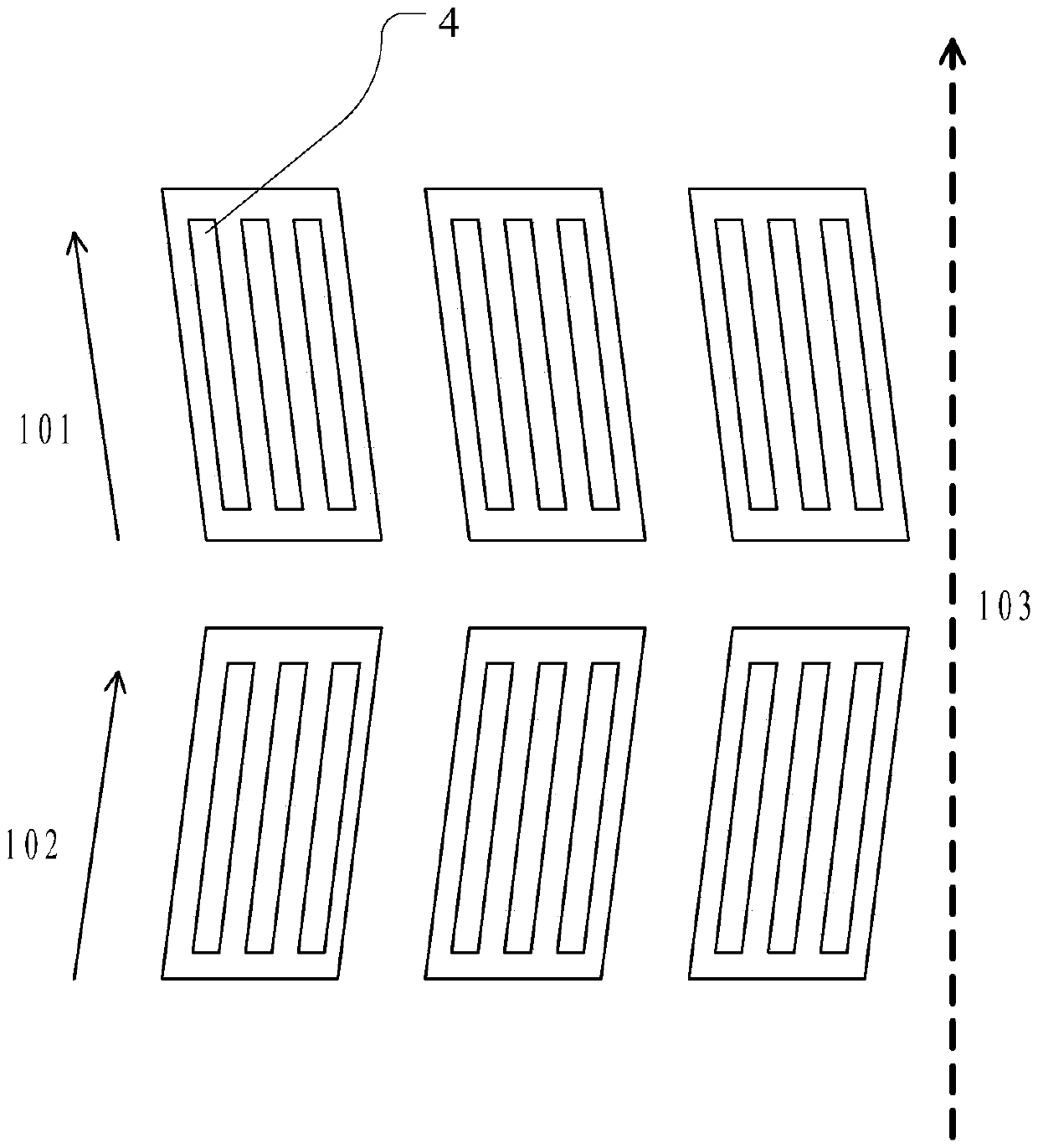
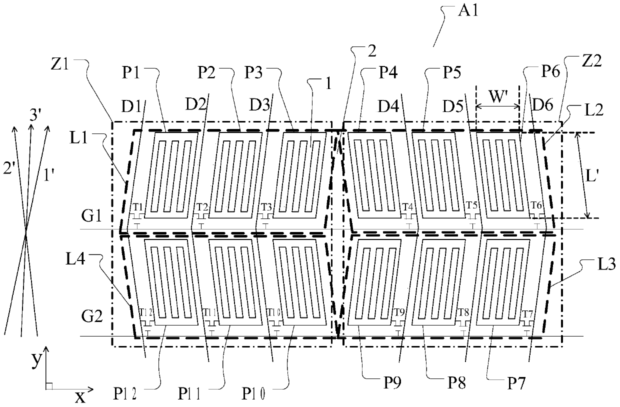
[0037] An embodiment of the present invention provides an array substrate, including: a plurality of pixel units, such as figure 2 as shown, figure 2 It is a schematic structural diagram of a pixel unit provided in Embodiment 1 of the present invention. The pixel unit A1 includes a matrix of 2×2 sub-pixel regions, and the matrix of 2×2 sub-pixel regions is arranged in a clockwise order as the first sub-pixel region L1, the second sub-pixel area L2, the third sub-pixel area L3 and the fourth sub-pixel area L4; the first sub-pixel area L1 and the fourth sub-pixel area L4 constitute the first group of pixel areas Z1, the second The sub-pixel area L2 and the third sub-pixel area L3 constitute a second group of pixel areas Z2; each of said sub-pixel areas includes at least three sub-pixels.

[0038] Each of the sub-pixels includes a strip-shaped electrode 1, and the strip-shaped electrodes in the first sub-pixel area L1 and the third sub-pixel area L3 are parallel to the first d...

Embodiment 2

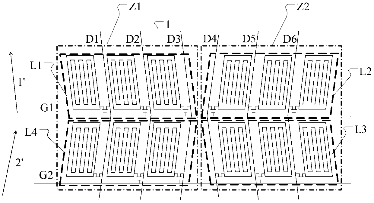
[0070] An embodiment of the present invention provides an array substrate, including: a plurality of pixel units, such as Figure 8 as shown, Figure 8 It is a schematic structural diagram of a pixel unit provided in Embodiment 2 of the present invention. The pixel unit A1 includes a matrix of 2×2 sub-pixel regions, and the matrix of 2×2 sub-pixel regions is arranged in a clockwise order as the first sub-pixel region L1, the second sub-pixel area L2, the third sub-pixel area L3 and the fourth sub-pixel area L4; the first sub-pixel area L1 and the fourth sub-pixel area L4 constitute the first group of pixel areas Z1, the second The sub-pixel area L2 and the third sub-pixel area L3 constitute a second group of pixel areas Z2; each of said sub-pixel areas includes four sub-pixels.

[0071] Each of the sub-pixels includes a strip electrode 1 and a slit 6, and the strip electrodes in the first sub-pixel area L1 and the third sub-pixel area L3 are aligned with the first direction 1...


PUM


Abstract

The invention discloses an array substrate, which includes a plurality of pixel units, and the pixel unit includes a 2×2 sub-pixel region matrix, and the 2×2 sub-pixel region matrix is ​​arranged in a clockwise order as the first sub-pixel region, the second sub-pixel region Two sub-pixel areas, a third sub-pixel area and a fourth sub-pixel area; each of the sub-pixel areas includes at least three sub-pixels; each of the sub-pixels includes a strip electrode; the first sub-pixel area and The strip electrodes in the third sub-pixel area are parallel to the first direction; the strip electrodes in the second sub-pixel area and the fourth sub-pixel area are parallel to the second direction; the The first direction and the second direction cross each other, and the angle between the first direction and the second direction is greater than 0 degrees and less than or equal to 90 degrees. The array substrate, display panel and display device provided in this embodiment can solve the problem of horizontal stripes, and can realize a wide viewing angle and improve the display effect of the panel.

Description

technical field [0001] The present invention relates to display technology, in particular to an array substrate, a display panel including the array substrate, and a display device including the display panel. Background technique [0002] The display panel has the advantages of thinness, low power consumption and low radiation, and is currently widely used in portable electronic products such as mobile phones and PDAs (Personal Digital Assistant, PDA), such as: Thin Film Transistor-Liquid Crystal Displays (Thin Film Transistor-Liquid Crystal Display, TFT-LCD), organic light emitting diode display (Organic Light Emitting Diode, OLED), low temperature polysilicon (Low Temperature Poly-silicon, LTPS) display and plasma display (Plasma Display Panel, PDP), etc. With the vigorous development of display technology, consumers have higher and higher requirements for display image quality. Consumers have increasingly higher requirements on viewing angle, color saturation, display e...

Claims


Application Information

Patent Timeline
Patent Type & Authority Patents(China)
IPC IPC(8): G02F1/1343G02F1/1335G02F1/1337
Inventor 金慧俊曹兆铿林珧李岩松王苗苗
Owner SHANGHAI AVIC OPTOELECTRONICS
Why Eureka
Try Eureka