Organic light-emitting device and manufacturing method of organic light-emitting device

An electroluminescence device and luminescence technology, which is applied in the direction of electric solid-state devices, semiconductor/solid-state device manufacturing, electrical components, etc. Reach 50-70% and other problems, achieve the effect of uniform luminous intensity, strong uniformity, and easy promotion and application

Inactive Publication Date: 2014-12-17
OCEANS KING LIGHTING SCI&TECH CO LTD +2
View PDF4 Cites 3 Cited by
  • Summary
  • Abstract
  • Description
  • Claims
  • Application Information

AI Technical Summary

Problems solved by technology

However, the commonly used cathode is a thin metal film, and its transmittance can only reach 50-70%.
The anode used is a transparent oxide film, and its transmittance can generally reach more than

Method used


Image

  • Organic light-emitting device and manufacturing method of organic light-emitting device
  • Organic light-emitting device and manufacturing method of organic light-emitting device
  • Organic light-emitting device and manufacturing method of organic light-emitting device

Examples


Embodiment Construction

[0036] The following will clearly and completely describe the technical solutions in the embodiments of the present invention with reference to the accompanying drawings in the embodiments of the present invention. Obviously, the described embodiments are only some, not all, embodiments of the present invention. Based on the embodiments of the present invention, all other embodiments obtained by persons of ordinary skill in the art without creative efforts fall within the protection scope of the present invention.

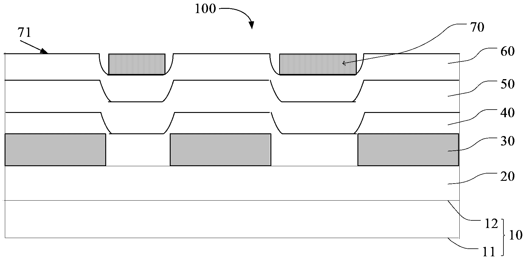
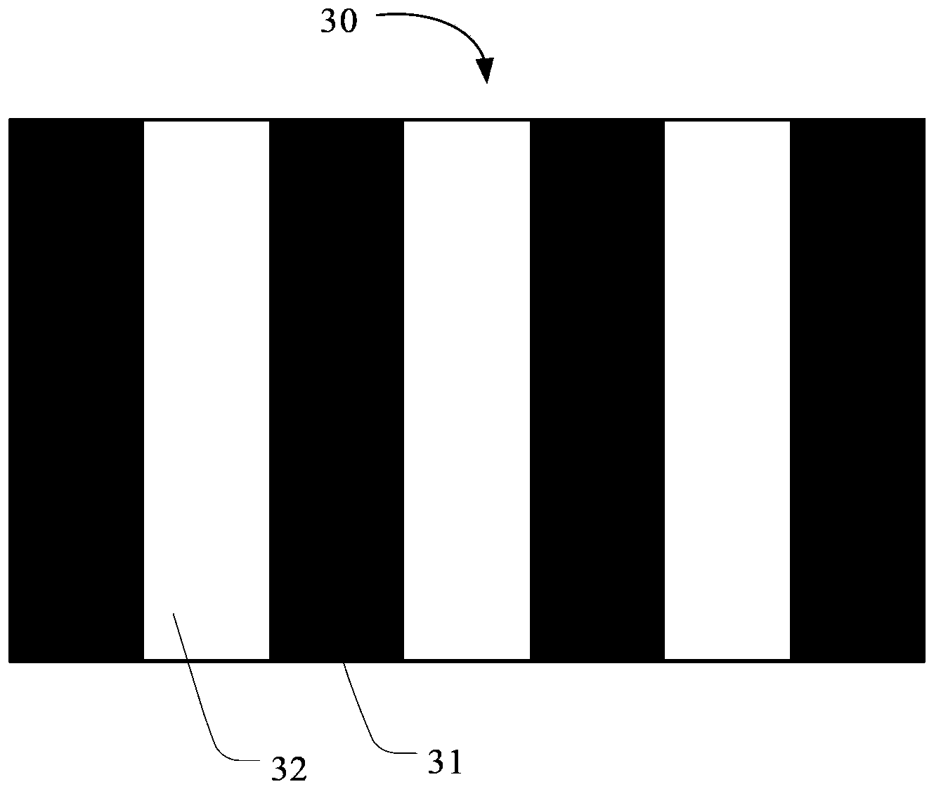
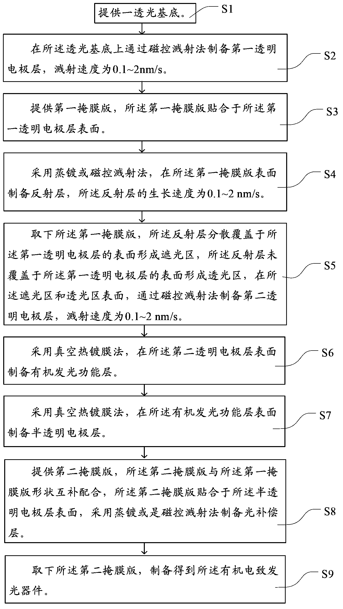
[0037] Embodiments of the present invention will be described below with reference to the accompanying drawings. see figure 1 , is a schematic structural diagram of an organic electroluminescent device 100 (OLED) in the first embodiment of the present invention. The organic electroluminescent device 100 includes a light-transmitting substrate 10, a first transparent electrode layer 20, a reflective layer 30, a second transparent electrode layer 40, an organic ligh...


PUM

PropertyMeasurementUnit
Thicknessaaaaaaaaaa
Thicknessaaaaaaaaaa
Thicknessaaaaaaaaaa

Abstract

The invention discloses an organic light-emitting device. The organic light-emitting device comprises a light-transmitting substrate, a first transparent electrode layer, a reflecting layer, a second transparent electrode layer, an organic light-emitting functional layer, a semitransparent electrode layer and a light compensating layer which are laminated in sequence, wherein the light-transmitting substrate comprises a first light-emitting surface and a covering surface which are arranged oppositely; the first transparent electrode layer covers the covering surface; the reflecting layer covers the surface of the first transparent electrode layer in a scattered manner, thereby forming a light-shielding region; the area ratio of the reflecting layer to the first transparent electrode layer is 20-80 percent; the surface of the reflecting layer not covering the first transparent electrode layer forms a light-transmitting region; the second transparent electrode layer covers the light-shielding region and the light-transmitting region; the organic light-emitting functional layer covers the surface of the second transparent electrode layer; the semitransparent electrode layer covers the surface of the organic light-emitting functional layer; and the light compensating layer only covers the surface of the semitransparent electrode layer corresponding to the light-transmitting region. The two light-emitting surfaces of the organic light-emitting device are uniform and consistent in light-emitting intensity. The invention further discloses a manufacturing method of the organic light-emitting device.

Description

technical field [0001] The invention relates to the field of light emitting devices, in particular to an organic electroluminescent device and a preparation method of the organic electroluminescent device. Background technique [0002] Organic Light Emission Diode (OLED) has the characteristics of high brightness, wide range of material selection, low driving voltage, full-cure active light emission, etc., and has the advantages of high definition, wide viewing angle, and fast response speed. A display technology and light source with great potential, in line with the development trend of mobile communication and information display in the information age, and the requirements of green lighting technology, is the focus of many researchers at home and abroad. [0003] Most of the existing organic electroluminescent technologies can only take out light from the anode or cathode side to produce bottom-emitting or top-emitting organic electroluminescent devices. The organic ele...

Claims


Application Information

Patent Timeline
IPC IPC(8): H01L51/50H01L51/52H01L51/56
CPCH10K77/10H10K50/816H10K50/856H10K71/00Y02E10/549Y02P70/50
Inventor 周明杰冯小明陈吉星王平
Owner OCEANS KING LIGHTING SCI&TECH CO LTD
Why Eureka
Try Eureka