Semiconductor light-emitting apparatus having multiple semiconductor light-emitting elements and its manufacturing method

a technology of semiconductor light-emitting elements and manufacturing methods, which is applied in the direction of basic electric elements, electrical devices, semiconductor devices, etc., can solve the problems of color unevenness among the semiconductor light-emitting elements and the inability to uniformize the and achieve the uniform illumination intensities the unevenness of the color of the semiconductor light-emitting elements.

Active Publication Date: 2019-06-06
STANLEY ELECTRIC CO LTD
View PDF0 Cites 1 Cited by
  • Summary
  • Abstract
  • Description
  • Claims
  • Application Information

AI Technical Summary

Benefits of technology

[0011]According to the presently disclosed subject matter, since the standard deviation σ1 of thicknesses of the transparent adhesive layers is small, the slopes of the semiconductor light-emitting elements caused by the eutectic process or thermally-pressuring process can be compensated for, and also, the heat resistances between the wavelength-converting plate and each of the semiconductor light-emitting elements can be uniform, so that luminance intensities of the semiconductor light-emitting elements can be uniform, and also, the color unevenness among the semiconductor light-emitting elements can be resolved.

Problems solved by technology

Thus, the heat resistances between the wavelength-converting plate and each of the semiconductor light-emitting elements would greatly fluctuate, so that luminance intensities of the semiconductor light-emitting elements would not be uniform, and also, the color unevenness among the semiconductor light-emitting elements would occur.

Method used


Image

  • Semiconductor light-emitting apparatus having multiple semiconductor light-emitting elements and its manufacturing method
  • Semiconductor light-emitting apparatus having multiple semiconductor light-emitting elements and its manufacturing method
  • Semiconductor light-emitting apparatus having multiple semiconductor light-emitting elements and its manufacturing method

Examples


first embodiment

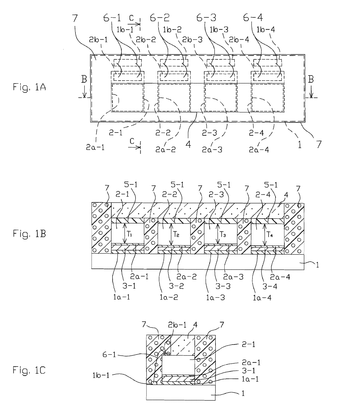
[0025]FIG. 1A is a plan view illustrating the semiconductor light-emitting apparatus according to the presently disclosed subject matter, FIG. 1B is a cross-sectional view taken along the line B-B in FIG. 1A, and FIG. 1C is a cross-sectional view taken along the line C-C in FIG. 1A.

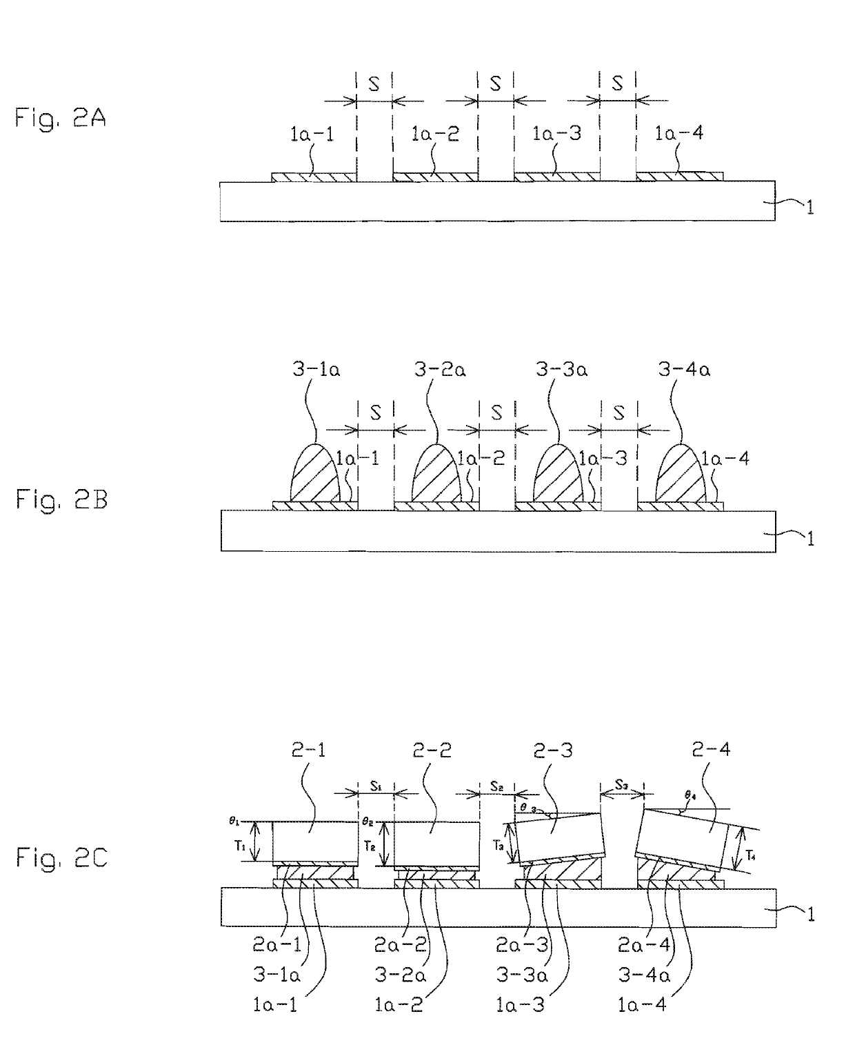
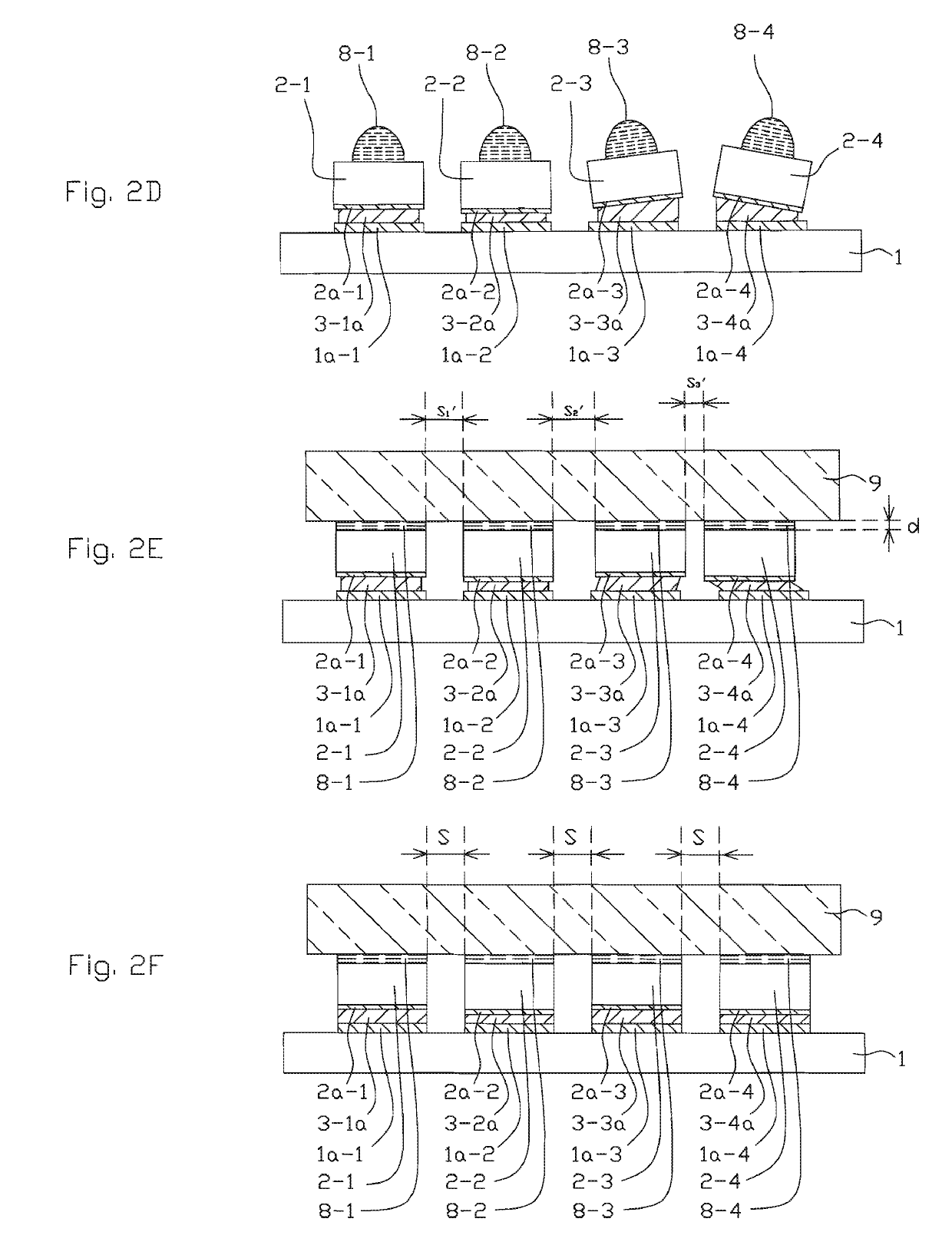
[0026]In FIGS. 1A, 1B and 1C, face-up type blue-light LED elements 2-1, 2-2, 2-3 and 2-4 are equidistantly mounted on a wiring substrate 1 via conductive eutectic layers 3-1, 3-2, 3-3 and 3-4, respectively. Also, a wavelength-converting plate 4 is mounted on upper surfaces of the LED elements 2-1, 2-2, 2-3 and 2-4 via transparent adhesive layers 5-1, 5-2, 5-3 and 5-4.

[0027]The substrate 1 has four p-side electrode patterns 1a-1, 1a-2, 1a-3 and 1a-4 and n-side electrode pads 1b-1, 1b-2, 1b-3 and 1b-4 on the upper surface. On the other hand, the LED elements 2-1, 2-2, 2-3 and 2-4 have p-side electrode patterns 2a-1, 2a-2, 2a-3 and 2a-4 on the lower surface and n-side electrode pads 2b-1, 2b-2, 2b-3 and 2b-4...

second embodiment

[0069]FIG. 4A is a plan view illustrating the semiconductor light-emitting apparatus according to the presently disclosed subject matter, FIG. 4B is a cross-sectional view taken along the line B-B in FIG. 4A, and FIG. 4C is a bottom view of the LED elements of FIG. 4A.

[0070]In FIGS. 4A, 4B and 4C, face-down type blue-light LED elements 2′-1, 2′-2, 2′-3 and 2′-4 are provided instead of the face-down type blue-light LED elements 2-1, 2-2, 2-3 and 2-4, respectively, of FIGS. 1A, 1B and 1C.

[0071]The substrate 1 has n-side electrode patterns 1b′-1, 1b′-2, 1b′-3 and 1b′-4 instead of the n-side electrode pads 1b-1, 1b-2, 1b-3 and 1b-4, respectively, of FIGS. 1A, 1B and 1C. On the other hand, the LED elements 2′-1, 2′-2, 2′-3 and 2′-4 has n-side electrode patterns 2b′-1, 2b′-2, 2b′-3 and 2b′-4 on its lower surface corresponding to the n-side electrode patterns 1b′-1, 1b′-2, 1b′-3 and 1b′-4, respectively. In this case, the area of each of the n-side electrode patterns 2b′-1, 2b′-2, 2b′-3 and...


PUM


Abstract

A semiconductor light-emitting apparatus includes: a wiring substrate; multiple semiconductor light-emitting elements mounted via multiple eutectic layers, respectively, on the wiring substrate; and a wavelength-converting plate via multiple transparent adhesive layers on upper surfaces of the semiconductor light-emitting elements, respectively. A standard deviation of thicknesses of the transparent adhesive layers is smaller than a standard deviation of thicknesses of the eutectic layers.

Description

[0001]This application claims the priority benefit under 35 U.S.C. § 119 to Japanese Patent Application No. JP2017-234000 filed on Dec. 6, 2017, which disclosure is hereby incorporated in its entirety by reference.BACKGROUNDField[0002]The presently disclosed subject matter relates to a semiconductor light-emitting apparatus such as a white-light light-emitting diode (LED) apparatus and its manufacturing method.Description of the Related Art[0003]Generally, a semiconductor light-emitting apparatus such as a white-light LED apparatus is used as an illumination apparatus such as a vehicle headlamp, a street lamp or a conventional lamp.[0004]A prior art semiconductor light-emitting apparatus is constructed by a wiring substrate, a semiconductor light-emitting element mounted via a conductive eutectic layer on the substrate, and a wavelength-converting plate such as a phosphor plate adhered to the upper surface of the semiconductor light-emitting element via a transparent adhesive layer....

Claims


Application Information

Patent Timeline
Patent Type & Authority Applications(United States)
IPC IPC(8): H01L33/62H01L25/075H01L33/60
CPCH01L33/62H01L25/0753H01L33/60H01L2933/0066H01L33/505H01L33/54H01L33/56H01L2933/0041H01L2933/005
Inventor HARADA, MITSUNORITACHIBANA, KAORI
Owner STANLEY ELECTRIC CO LTD
Why Eureka
Try Eureka