Silk-screen printing device and silk-screen printing method

A screen printing device and screen technology, which is applied to screen printing machines, printing machines, printing machines, etc., can solve problems such as the influence of the tin leakage rate, and achieve the goal of improving the tin leakage rate, reducing the amount of solder paste, and reducing the number of times Effect

Inactive Publication Date: 2015-03-25
SAMSUNG SEMICON CHINA RES & DEV +1
View PDF6 Cites 0 Cited by
  • Summary
  • Abstract
  • Description
  • Claims
  • Application Information

AI Technical Summary

Problems solved by technology

[0004] However, for traditional screen printing technology, the solder leakage rate is affected by the material of the screen stencil and the size of the opening of the screen stencil

Method used


Image

  • Silk-screen printing device and silk-screen printing method
  • Silk-screen printing device and silk-screen printing method
  • Silk-screen printing device and silk-screen printing method

Examples


Embodiment Construction

[0020] The invention will be described in more detail hereinafter with reference to the accompanying drawings, in which exemplary embodiments of the invention are shown. It should be understood by those skilled in the art that these examples are provided in an illustrative sense only and should not be construed as limiting the scope of the present invention. Rather, these embodiments are provided so that this disclosure will be thorough and complete, and will fully convey the scope of the invention to those skilled in the art.

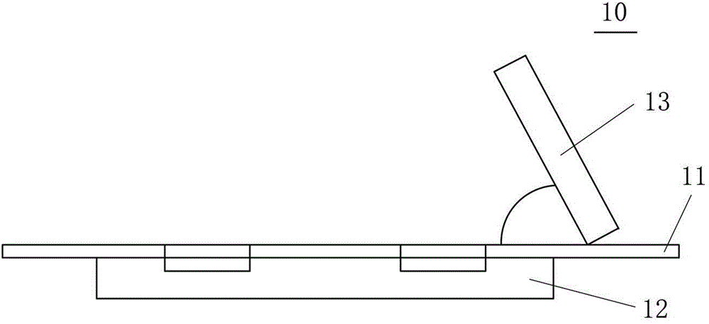
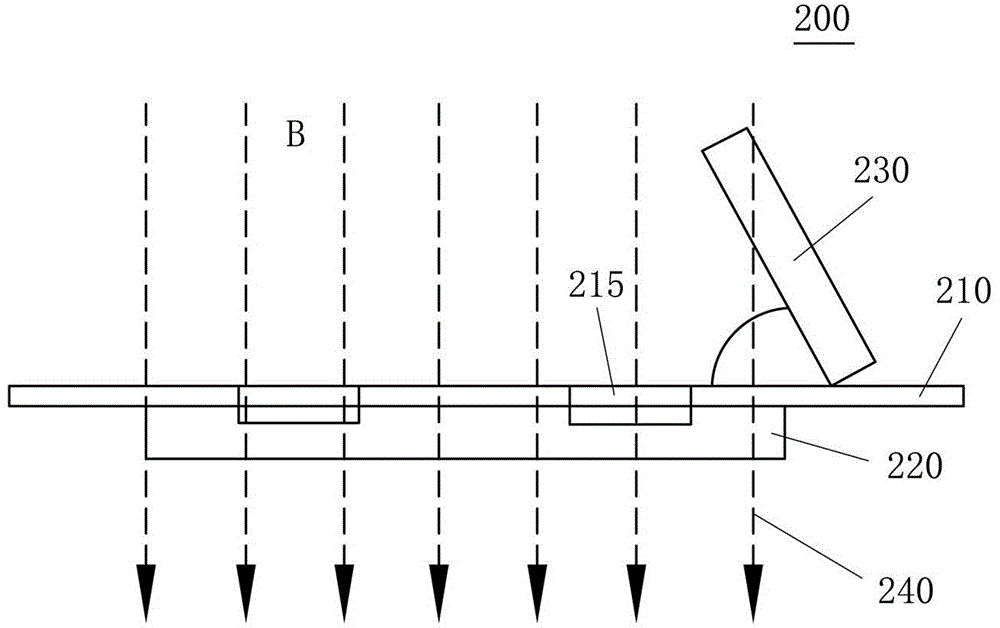
[0021] figure 2 is a schematic diagram showing a screen printing apparatus according to an exemplary embodiment of the present invention.

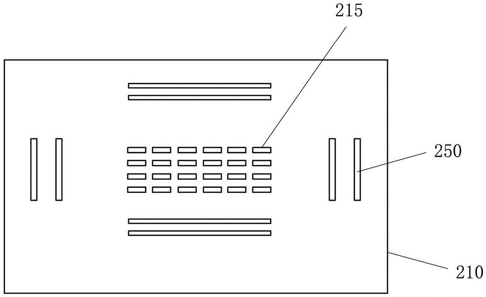
[0022] refer to figure 2 , the screen printing device 200 according to an exemplary embodiment of the present invention may include: a screen stencil 210 having patterned openings 215; a scraper 230 used to scrape back and forth the solder paste positioned on the screen stencil 210 to Solder paste is located i...


PUM


Abstract

The invention provides a silk-screen printing device and a silk-screen printing method. The silk-screen printing device comprises a silk-screen printing template and a scraper blade, the silk-screen printing template is provided with a patterned opening and located in an alternating magnetic field, the scraper blade moves back and forth on the silk-screen printing template in a scraping mode, and silk-screen printing materials on the silk-screen printing template are arranged in the patterned opening. Magnetic materials or materials capable of being magnetized are attached to the silk-screen printing template, the direction of the magnetic field intensity of the alternating magnetic field is perpendicular to the horizontal face of the silk-screen printing template, and the magnetic field intensity of the alternating magnetic field changes in the perpendicularly-upward direction or the perpendicularly-downward direction.

Description

technical field [0001] The invention relates to the field of screen printing of semiconductor devices, more specifically, to a screen printing device using an alternating magnetic field and a screen printing method. Background technique [0002] As electronic devices get smaller, the openings of the stencils become smaller, which reduces the amount of solder paste printed. In order to increase the amount of solder paste on the circuit board, it is necessary to increase the tin leakage rate of the solder paste. [0003] figure 1 is a schematic diagram showing a conventional screen printing apparatus 10. refer to figure 1 The screen stencil 11 is located on the circuit board 12, and the scraper 13 is used to scrape back and forth the solder paste on the screen stencil 11, so that the solder paste passes through the opening of the screen stencil 11 and is located on the circuit board 12, thereby completing the printing. [0004] However, for traditional screen printing tech...

Claims


Application Information

Patent Timeline
IPC IPC(8): B41F15/08B41F15/34
Inventor 王玉传
Owner SAMSUNG SEMICON CHINA RES & DEV
Why Eureka
Try Eureka