Die sinking and printing mechanism of circuit board

A printing mechanism and circuit board technology, applied in the direction of assembling printed circuits with electrical components, to improve product quality, reduce the amount of solder paste, and overcome the effects of component bridging

Pending Publication Date: 2018-01-30
FLEXTRONICS ELECTRONICS TECH SUZHOU
View PDF0 Cites 0 Cited by
  • Summary
  • Abstract
  • Description
  • Claims
  • Application Information

AI Technical Summary

Problems solved by technology

[0003] The main technical problem to be solved by the present invention is to provide a printing mechanism for circuit board mold opening. Using the groove on the back of the printing template corresponding to the position of the splint, it can effectively reduce the amoun

Method used


Image

  • Die sinking and printing mechanism of circuit board

Examples


Embodiment Construction

[0017] The following will clearly and completely describe the technical solutions in the embodiments of the present invention. Obviously, the described embodiments are only some of the embodiments of the present invention, rather than all the embodiments. Based on the embodiments of the present invention, all other embodiments obtained by persons of ordinary skill in the art without making creative efforts belong to the protection scope of the present invention.

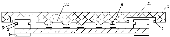
[0018] see figure 1 , the embodiment of the present invention includes:

[0019] A printing mechanism for circuit board mold opening, comprising: a board-feeding track 1, a splint 2, a printing template 3, and a scraper arranged above the printing template 3, and two board-feeding tracks 1 are respectively arranged on the line On the upper and lower sides of the board, the clamping device 2 is arranged above the board entry track 1 and clamps and fixes the circuit board. The printing template 3 includes a groove par...


PUM


Abstract

The invention discloses a die sinking and printing mechanism of a circuit board. The mechanism comprises board feeding tracks, board clamping devices, a printing template, and a scraper arranged abovethe printing template. The two board feeding tracks are arranged at the upper side and the lower side of the circuit board; the board clamping devices are arranged above the board feeding tracks andare used for clamping and fixing the circuit board tightly. The printing template consists of a groove part and a middle printing part; and the printing template is installed above the board clampingdevices by the groove part. With the method disclosed by the invention, the solder paste amount in the printing area close to the board clamping device is reduced and a problem of bridge connection ofcomponents close to a narrow edge region on the narrow-process-edge printed circuit board is solved; the operation links in production are reduced; and the product quality is improved.

Description

technical field [0001] The invention relates to the field of electronic circuit board printing devices, in particular to a mold opening and printing mechanism for circuit boards. Background technique [0002] In the design of printed circuit boards, due to cost savings, the process edge is narrow, and the splint of the printing machine clamps the edge of the printed circuit board, which is closer to the printing area. There is more solder paste residue in the printing area near the splint. After reflow soldering of electronic components, bridging occurs, and there are many operating links in production, and the product quality is low. Contents of the invention [0003] The main technical problem to be solved by the present invention is to provide a printing mechanism for circuit board mold opening. Using the groove on the back of the printing template corresponding to the position of the splint, it can effectively reduce the amount of solder paste near the printing area of...

Claims


Application Information

Patent Timeline
IPC IPC(8): H05K3/34
Inventor 乔辉张俊赵飞
Owner FLEXTRONICS ELECTRONICS TECH SUZHOU
Why Eureka
Try Eureka