Detector and preparation method thereof and emission imaging device with the same

A technology of imaging equipment and detectors, applied in instruments, measuring devices, scientific instruments, etc., can solve the problems of increasing crystal decoding errors, difficult to control precision, and affecting the imaging quality of the system, so as to control decoding errors, reduce influence, The effect of increasing the spatial resolution of an image

Active Publication Date: 2015-05-06
DONGGUAN SONGSHAN LAKE SOUTHEN MEDICAL UNIV SCI & TECH PARK CO LTD
View PDF12 Cites 10 Cited by
  • Summary
  • Abstract
  • Description
  • Claims
  • Application Information

AI Technical Summary

Problems solved by technology

[0007] Considering the above factors, the processing of the detector is very difficult and the accuracy is difficult to control
Insufficient processing and assembly precision usually cause a significant increase in crystal decoding errors, seriously affecting the imaging quality of the system

Method used


Image

  • Detector and preparation method thereof and emission imaging device with the same
  • Detector and preparation method thereof and emission imaging device with the same
  • Detector and preparation method thereof and emission imaging device with the same

Examples


Embodiment Construction

[0049] In the following description, numerous specific details are given in order to provide a more thorough understanding of the present invention. It will be apparent, however, to one skilled in the art that the present invention may be practiced without one or more of these details. In other examples, some technical features known in the art are not described in order to avoid confusion with the present invention.

[0050] In order to provide a thorough understanding of the present invention, the detailed structure will be set forth in the following description. Obviously, the embodiments of the invention are not limited to specific details familiar to those skilled in the art. Preferred embodiments of the present invention are described in detail below, however, the present invention may have other embodiments besides these detailed descriptions.

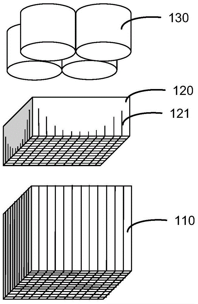
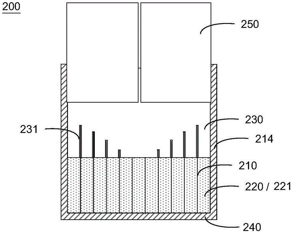
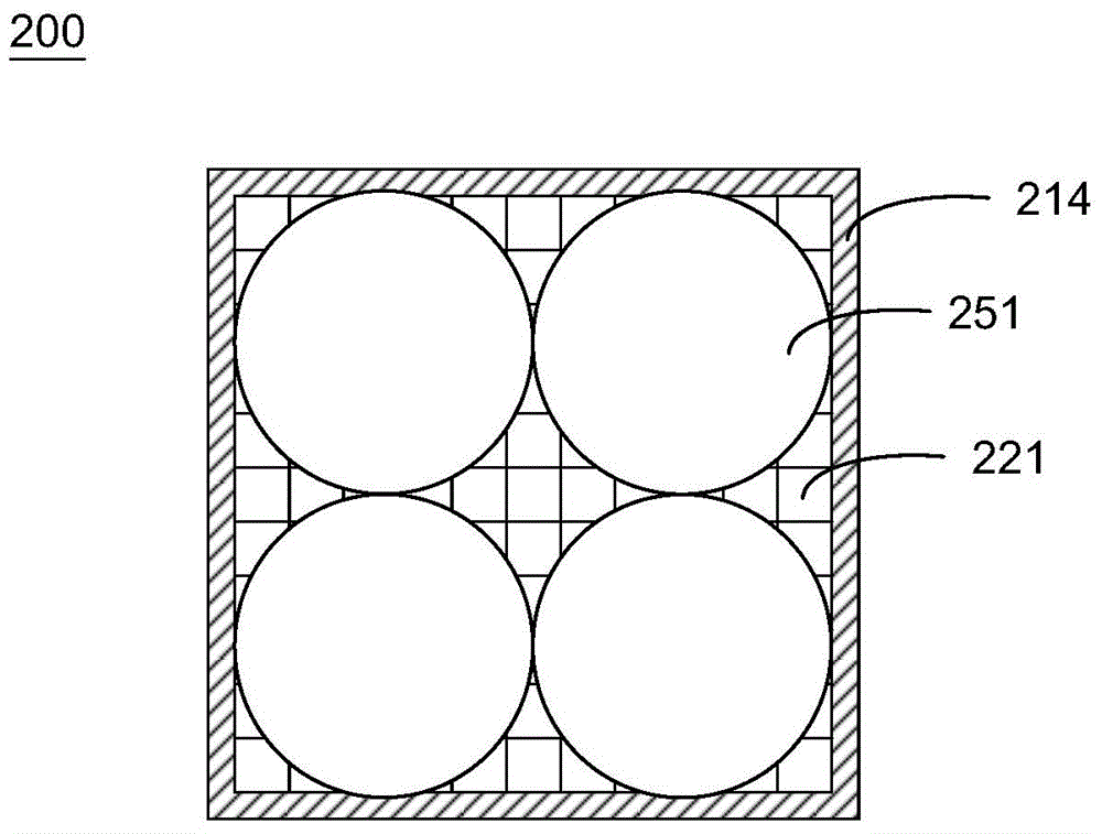
[0051] The present invention provides a detector for an emission imaging device. Such as Figure 2A-2B As shown, the detec...


PUM


Abstract

The invention provides a detector and a preparation method of the detector and an emission imaging device with the detector. The detector comprises a grid mold, a crystal layer and a solid photoconductive layer. The grid mold comprises multiple transverse walls, multiple longitudinal walls and a peripheral frame encircles the walls from side direction, wherein the transverse walls and the longitudinal walls are respectively arranged along the transverse direction and the longitudinal direction in an intersection mode so that multiple grid grooves which are arranged in a matrix mode are formed in the peripheral frame. The crystal layer comprises multiple scintillation crystals arranged in a matrix mode, wherein the multiple scintillation crystals and the multiple grid grooves are correspondingly fixed in the multiple grid grooves one by one, and the top surfaces of the multiple transverse walls and the multiple longitudinal walls are not lower than that of the crystal layer. The solid photoconductive layer is arranged on the top surface of the crystal layer and provided with a cutting groove, and the portions of the multiple transverse walls and the multiple longitudinal walls which are higher than the crystal layer are inserted into the cutting groove. The detector effectively controls the decoding errors of crystals and improves the resolution ratio of the image space of an emission imaging device.

Description

technical field [0001] The present invention relates to an emission imaging system, in particular to a detector for an emission imaging device and a manufacturing method thereof, and also to an emission imaging device with the detector. Background technique [0002] Emission imaging technologies such as Positron Emission Tomography (PET) and Single-Photon Emission Computed Tomography (SPECT) have been used in medical diagnosis, pathology research, pharmacology research, drug development and other fields. [0003] Taking positron emission imaging as an example, it uses the phenomenon that the positrons produced by the decay of positron isotopes and the negative electrons in the human body have an annihilation effect. The detector is used to detect the gamma photons produced by the annihilation effect to obtain the distribution information of isotopes in the human body, and the computer performs reconstruction and combination operations to obtain a three-dimensional tomograph...

Claims


Application Information

Patent Timeline
IPC IPC(8): G01T1/202
Inventor 石涵许剑锋彭旗宇
Owner DONGGUAN SONGSHAN LAKE SOUTHEN MEDICAL UNIV SCI & TECH PARK CO LTD
Why Eureka
Try Eureka