Pixel defining layer and its preparation method, display substrate and its preparation method, display device

A pixel definition layer and substrate technology, applied in semiconductor/solid-state device manufacturing, organic semiconductor devices, electrical components, etc., can solve the problems of not keeping performance for too long and failure

Active Publication Date: 2017-05-31
BOE TECH GRP CO LTD
View PDF4 Cites 0 Cited by
  • Summary
  • Abstract
  • Description
  • Claims
  • Application Information

AI Technical Summary

Problems solved by technology

In order to realize the liquid repellency of the pixel defining layer 20, the most conventional liquid repelling treatment method is to perform fluorine-containing plasma treatment on the basic pattern of the above pixel defining layer. However, due to the characteristics of plasma, its performance is generally not maintained for too long , so that in the face of a longer process process or a higher temperature annealing process, failure problems may occur

Method used


Image

  • Pixel defining layer and its preparation method, display substrate and its preparation method, display device
  • Pixel defining layer and its preparation method, display substrate and its preparation method, display device
  • Pixel defining layer and its preparation method, display substrate and its preparation method, display device

Examples


Embodiment Construction

[0035] The technical solutions in the embodiments of the present invention will be clearly and completely described below with reference to the accompanying drawings in the embodiments of the present invention. Obviously, the described embodiments are only a part of the embodiments of the present invention, but not all of the embodiments. Based on the embodiments of the present invention, all other embodiments obtained by those of ordinary skill in the art without creative efforts shall fall within the protection scope of the present invention.

[0036] An embodiment of the present invention provides a method for preparing a pixel definition layer, the method comprising:

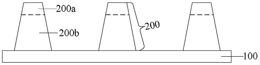
[0037] S01, such as Figure 3a As shown, a basic pixel definition layer pattern 200 is formed on the substrate 100; the basic pixel definition layer pattern 200 includes a first pattern 200a of an inorganic material, and the first pattern 200a is located at the highest point of the basic pattern 200 of the p...


PUM


Abstract

Embodiments of the present invention provide a pixel defining layer and its preparation method, a display substrate and its preparation method, and a display device, which relate to the field of display technology and can maintain the lyophobic property of the pixel defining layer for a long time. The preparation method of the pixel defining layer includes: forming a basic pattern of the pixel defining layer on a substrate; the basic pattern of the pixel defining layer includes a first pattern of an inorganic material, and the first pattern is located at the base of the basic pattern of the pixel defining layer Topmost: performing self-assembled monomolecular layer surface treatment on the first pattern to form a fluorinated monomolecular layer on the surface of the first pattern to form the pixel defining layer. For any display device that can be manufactured using inkjet printing.

Description

technical field [0001] The present invention relates to the field of display technology, and in particular, to a pixel defining layer and a preparation method, a display substrate and a preparation method, and a display device. Background technique [0002] In recent years, researchers have begun to try to apply inkjet printing technology to the preparation of planar functional materials, such as the preparation of organic material functional layers for organic electroluminescent diode displays, and color filter layers for liquid crystal displays. [0003] Take organic electroluminescent diode displays (OLEDs) as an example, such as figure 1 and figure 2 As shown, the organic electroluminescent diode includes a pixel area 01 and a non-pixel area 02, and the pixel area 01 is composed of a plurality of pixels 10, wherein each pixel 10 includes an anode, an organic material functional layer and a cathode( figure 1 and figure 2 are not identified). Wherein, when the organ...

Claims


Application Information

Patent Timeline
Patent Type & Authority Patents(China)
IPC IPC(8): H01L51/56H01L51/52H01L27/32
CPCH10K59/00H10K59/122H10K71/191H10K71/20H10K59/173H10K85/60H10K85/40H10K59/1201H10K2102/00H10K71/00
Inventor 石守磊刘则
Owner BOE TECH GRP CO LTD
Why Eureka
Try Eureka