Eureka AIR delivers breakthrough ideas for toughest innovation challenges, trusted by R&D personnel around the world.

Optical imaging lens and electronic device using the optical imaging lens

An optical imaging lens and imaging technology, applied in the field of optical lenses, can solve problems related to material characteristics, achieve the effects of light, thin and small structure design, overcome aberrations, and good practical performance

Active Publication Date: 2017-11-10
GENIUS ELECTRONICS OPTICAL XIAMEN
View PDF4 Cites 0 Cited by
  • Summary
  • Abstract
  • Description
  • Claims
  • Application Information

AI Technical Summary

Problems solved by technology

[0003] However, the design of optical imaging lens is not simply to scale down the lens with good imaging quality to produce an optical imaging lens with both imaging quality and miniaturization. practical problems

Method used


Image

  • Optical imaging lens and electronic device using the optical imaging lens
  • Optical imaging lens and electronic device using the optical imaging lens
  • Optical imaging lens and electronic device using the optical imaging lens

Examples


Embodiment Construction

[0103] The present invention will now be further described with reference to the drawings and specific embodiments. Before the present invention is described in detail, it should be noted that in the following description, similar components are represented by the same numbers.

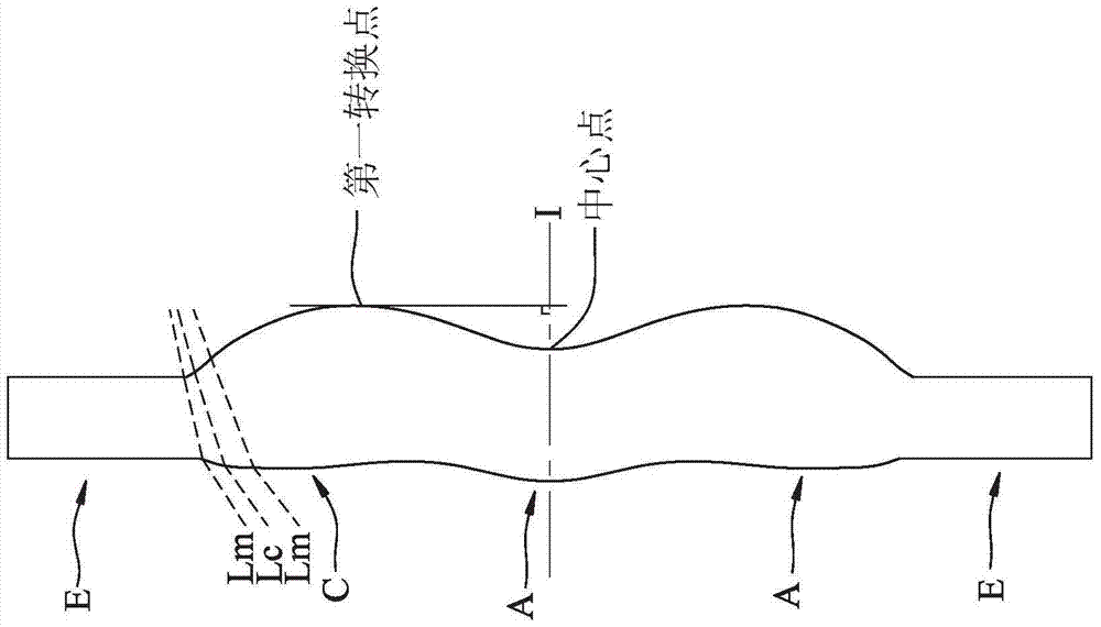
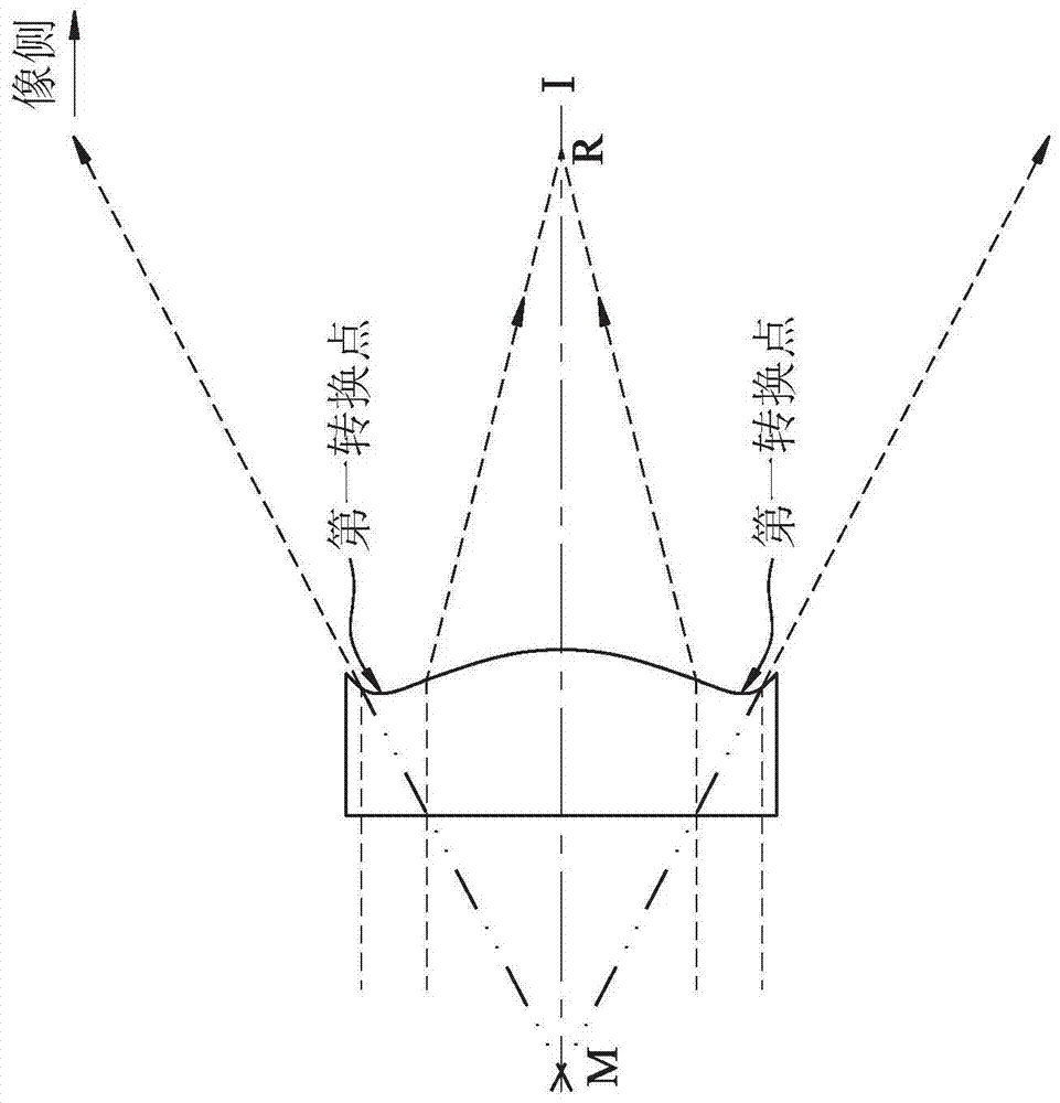
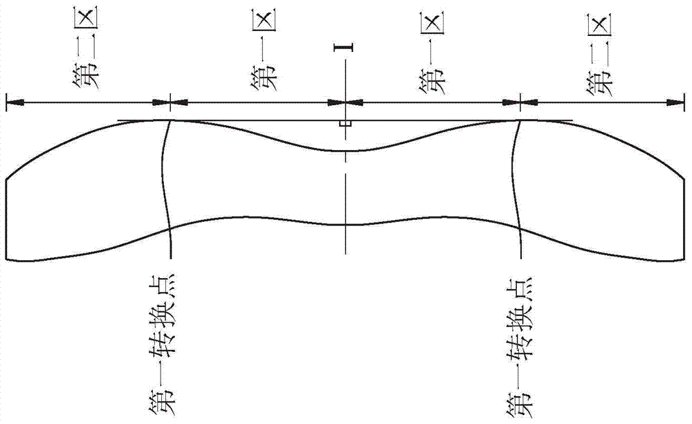
[0104] As used in this specification, "a lens has positive refractive power (or negative refractive power)" refers to the positive (or negative) refractive power on the optical axis of the lens calculated by Gaussian optics theory. The image side and object side are defined as the range through which the imaging light passes. The imaging light includes chief ray Lc and marginal ray Lm, such as figure 1 As shown, I is the optical axis and this lens is radially symmetrical with the optical axis I as the symmetry axis. The area where light passes through the optical axis is the area near the optical axis A, and the area where the edge light passes is the area near the circumference C. In addition, the lens ...


PUM


Abstract

The invention relates to an optical imaging lens and an electronic device using the optical imaging lens. The optical imaging lens includes four lenses, the image side of the first lens has a convex portion located in the vicinity of the optical axis; the object side of the second lens has a convex portion located in the vicinity of the optical axis, the second lens The image side has a convex portion located in the vicinity of the circumference; the image side of the third lens has a concave portion located in the vicinity of the circumference; and the image side of the fourth lens has a concave portion located in the vicinity of the optical axis , and a convexity in the vicinity of the circumference. The electronic device includes a casing; and an image module, which is installed in the casing, and includes the optical imaging lens, a lens barrel for the optical imaging lens, and a lens barrel for the lens barrel. A modular rear seat unit, and an image sensor arranged on the image side of the optical imaging lens. The invention provides better imaging quality under the condition of shortening the system length.

Description

Technical field [0001] The invention relates to an optical lens, in particular to an optical imaging lens and an electronic device using the optical imaging lens. Background technique [0002] In recent years, the popularization of portable electronic products such as mobile phones and digital cameras has led to the rapid development of image module related technologies. The image module mainly includes components such as optical imaging lenses, module holder units, and sensors. The trend toward thinner and lighter digital cameras has also increased the demand for miniaturization of image modules. With the development of Charge Coupled Device (CCD) or Complementary Metal-Oxide Semiconductor (Complementary Metal-Oxide Semiconductor) Due to the technological advancement and size reduction of CMOS), the optical imaging lens mounted in the image module also needs to be shortened correspondingly. However, in order to avoid the degradation of photographic effects and quality, the optic...

Claims


Application Information

Patent Timeline
Patent Type & Authority Patents(China)
IPC IPC(8): G02B13/18G02B13/00
CPCG02B13/004G02B7/021G02B9/34G02B9/36
Inventor 江依达林文斌公金辉
Owner GENIUS ELECTRONICS OPTICAL XIAMEN
Why Eureka
Eureka Blog
Learn More