
Contact Image Sensor Package Structure

A technology of image sensor and packaging structure, applied in image communication, electrical components, etc., can solve the problems of low assembly yield, increase the difficulty of assembly process, and high rework rate, and achieve the goal of simplifying assembly difficulty, improving work efficiency and yield rate Effect

Active Publication Date: 2018-06-12
NANTONG FUJITSU MICROELECTRONICS
View PDF4 Cites 0 Cited by
  • Summary
  • Abstract
  • Description
  • Claims
  • Application Information

AI Technical Summary

Problems solved by technology

This increases the difficulty of the assembly process, resulting in problems such as low assembly yield and high rework rate.

Method used


Image

  • Contact Image Sensor Package Structure
  • Contact Image Sensor Package Structure

Examples


Embodiment Construction

[0008] The application will be further described in detail below in conjunction with the accompanying drawings and embodiments. It should be understood that the specific embodiments described here are only used to explain related inventions, rather than to limit the invention. It should also be noted that, for ease of description, only parts related to the invention are shown in the drawings.

[0009] It should be noted that, in the case of no conflict, the embodiments in the present application and the features in the embodiments can be combined with each other. The present application will be described in detail below with reference to the accompanying drawings and embodiments.

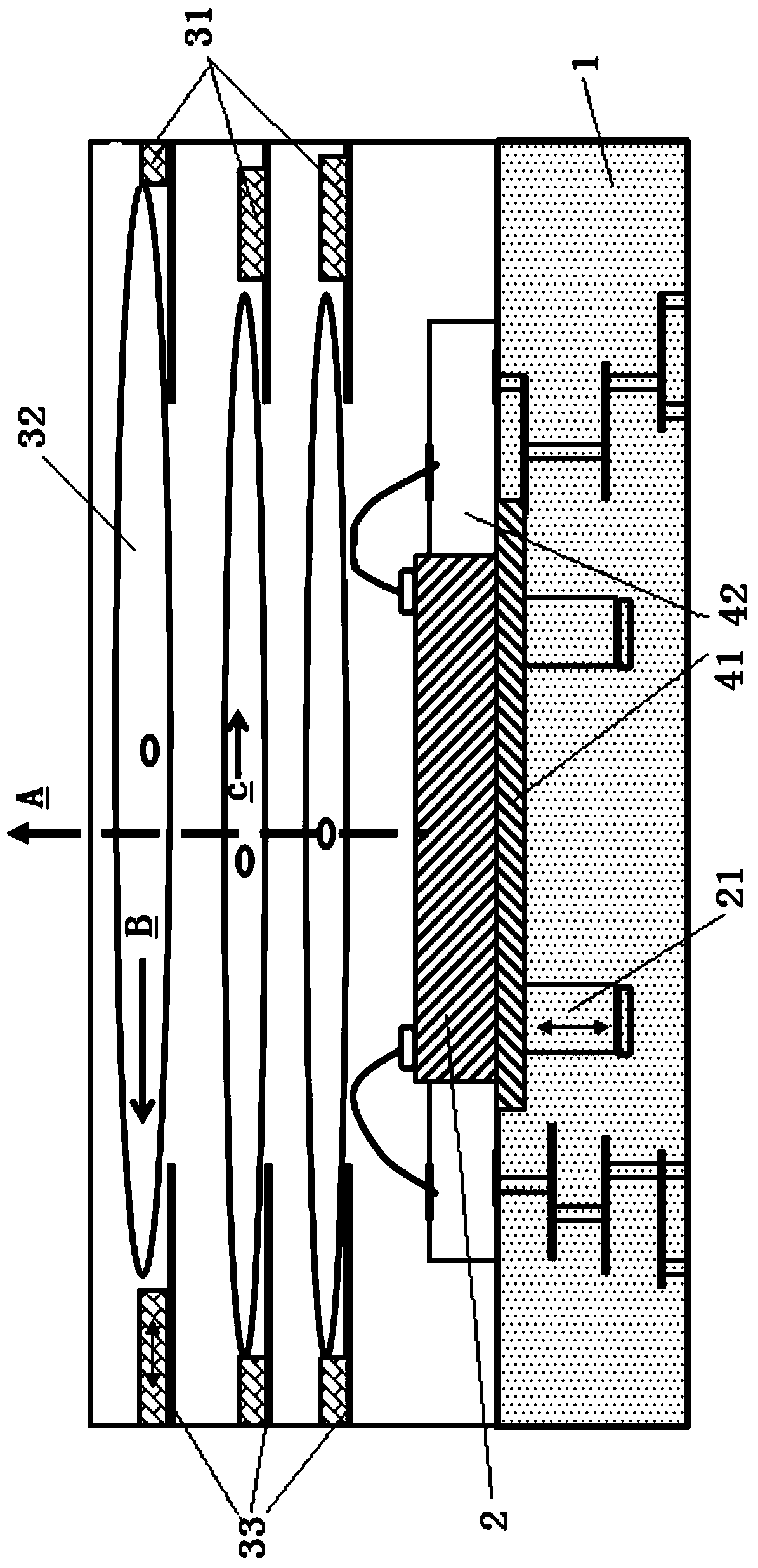
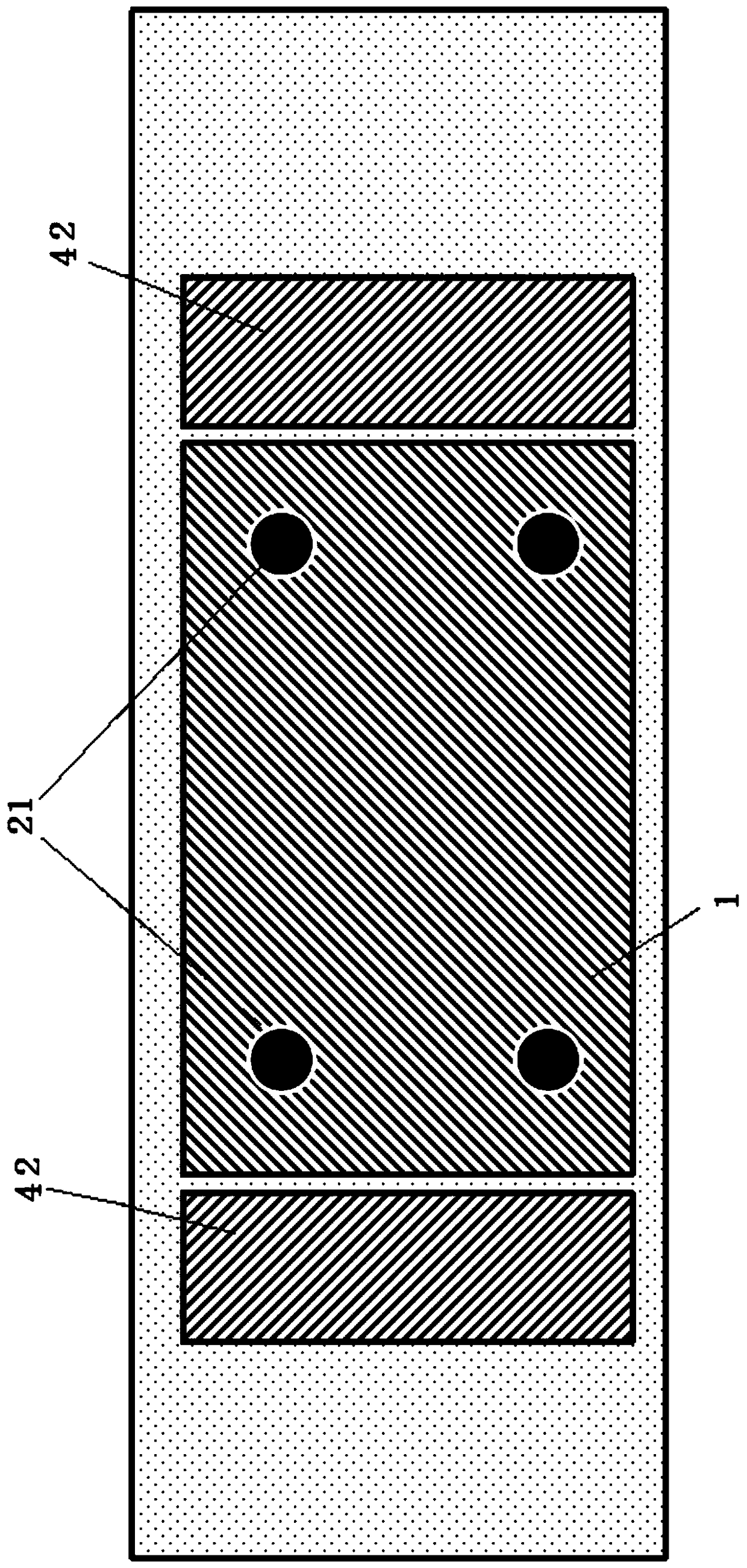
[0010] The invention discloses a contact image sensor packaging structure, such as figure 1 and figure 2 As shown, it includes a substrate 1, an image sensor chip 2 (hereinafter referred to as CIS chip 2), a mirror group, and an adjustment device. The adjustment device includes a first adjustmen...


PUM


Abstract

The invention discloses a contact-type image sensor packaging structure. The structure comprises a contact-type image sensor chip arranged on a substrate, a lens group arranged above the contact-type image sensor chip, a first adjusting apparatus and a second adjusting apparatus, wherein the first adjusting apparatus is arranged on the substrate and adjusts positions of the contact-type image sensor and the substrate; and the second adjusting apparatus is arranged on the lens group and adjusts a position of each lens in the lens group. Compared to the prior art, by using the structure of the invention, the first adjusting device and the second adjusting device adjust the positions of the contact-type image sensor chip and the lens group so that a confocal state of a lens group CIS chip and the lens group can be conveniently and rapidly realized, assembling difficulty is simplified, and operating efficiency and a yield are increased.

Description

technical field [0001] The present disclosure generally relates to chip modules, in particular to image sensors, and in particular to a contact image sensor packaging structure. Background technique [0002] In the packaging process of the contact image sensor (Contact Image Sensor, CIS) packaging structure, whether the CIS chip is in focus with the mirror group is an important part. The higher the resolution of the product, the higher the requirement for confocal during assembly. This increases the difficulty of the assembly process, resulting in problems such as low assembly yield and high rework rate. Contents of the invention [0003] In view of the above defects or deficiencies in the prior art, it is desired to provide a contact image sensor packaging structure, including: a contact image sensor chip arranged on a substrate, and a mirror group arranged above the contact image sensor chip, It also includes: a first adjustment device, arranged on the substrate, to ad...

Claims


Application Information

Patent Timeline
Patent Type & Authority Patents(China)
IPC IPC(8): H04N1/031
CPCH04N1/0313H04N1/0314
Inventor 丁万春
Owner NANTONG FUJITSU MICROELECTRONICS
Learn More