Pixel structure and array substrate and liquid crystal panel thereof

A pixel structure and liquid crystal panel technology, applied in nonlinear optics, instruments, optics, etc., can solve problems such as display gray scale changes, achieve the effects of reducing load and delay, reducing coupling capacitance, and reducing overlapping area

Inactive Publication Date: 2016-07-20
TCL CHINA STAR OPTOELECTRONICS TECH CO LTD
View PDF6 Cites 16 Cited by
  • Summary
  • Abstract
  • Description
  • Claims
  • Application Information

AI Technical Summary

Problems solved by technology

During the conversion process of the data line and the gate line voltage, the gray scale voltage of other pixel

Method used


Image

  • Pixel structure and array substrate and liquid crystal panel thereof
  • Pixel structure and array substrate and liquid crystal panel thereof
  • Pixel structure and array substrate and liquid crystal panel thereof

Examples


Embodiment Construction

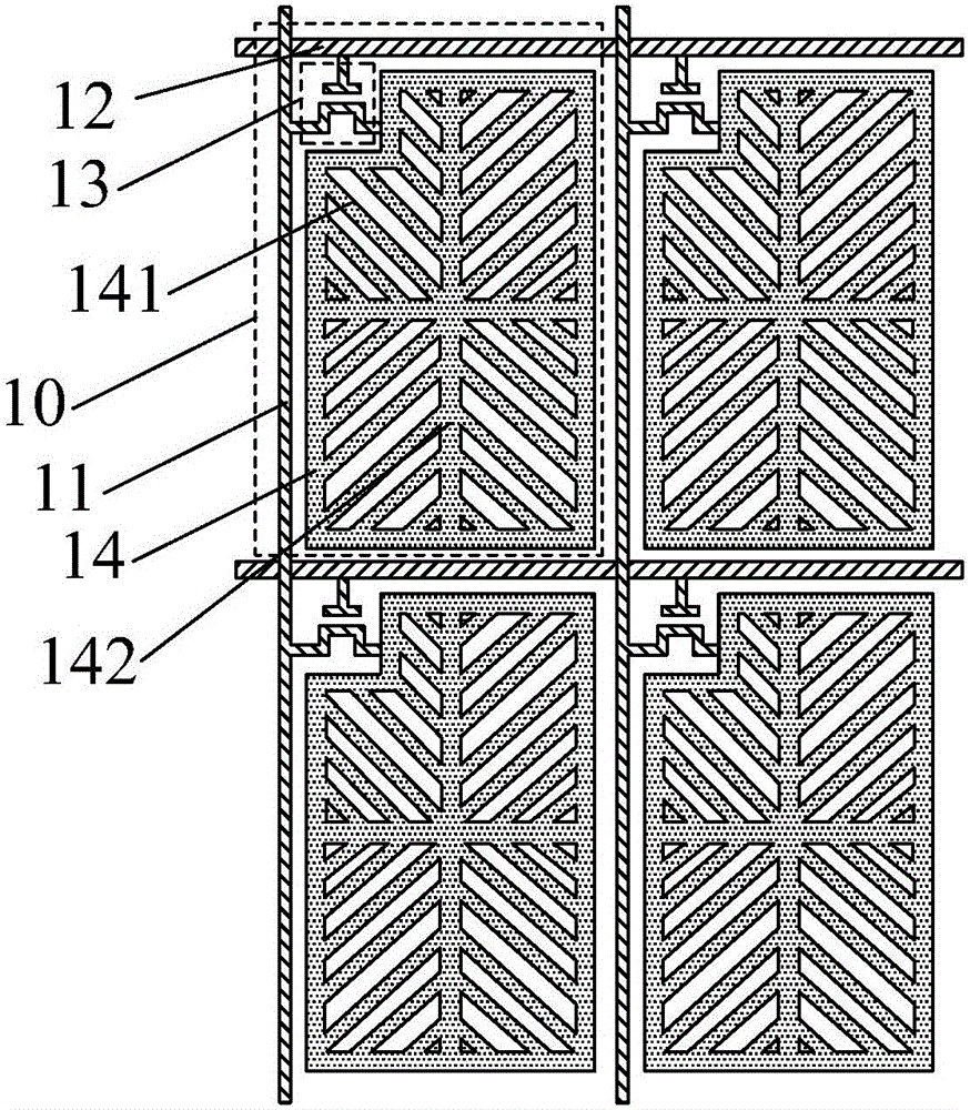
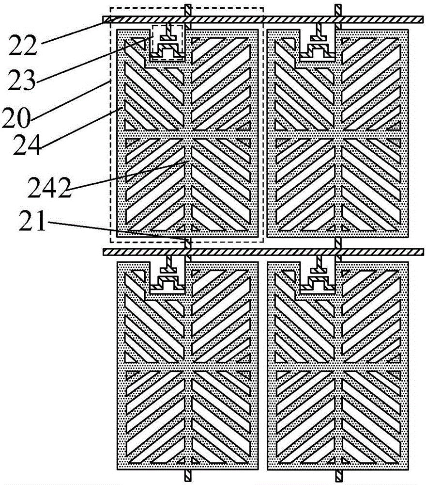
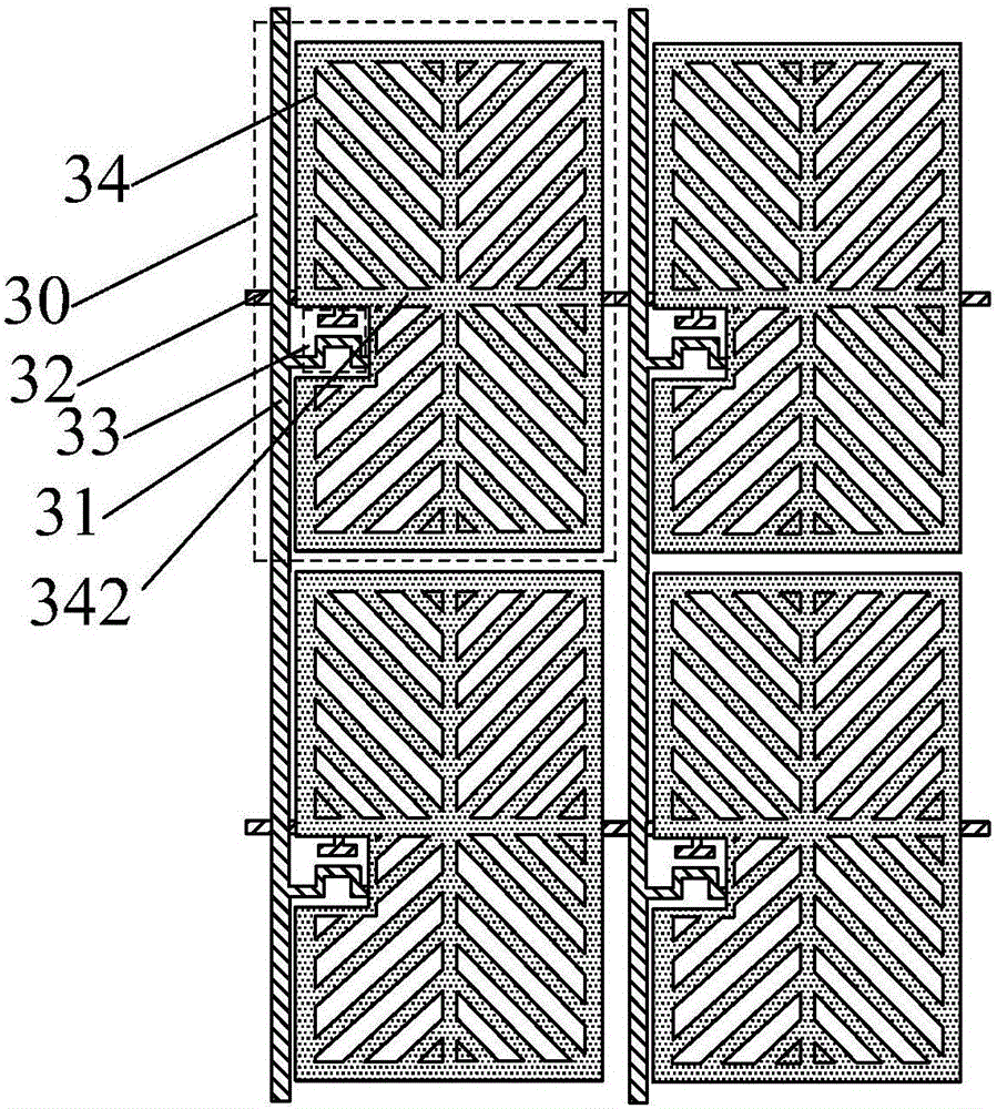
[0030] see Figure 4 , which is a schematic diagram of the first preferred embodiment of the pixel structure of the present invention. The pixel structure 40 mainly includes a data line 41 , a gate line 42 , a thin film transistor 43 , and a pixel electrode 44 including four domains distributed in double rows and double columns. and figure 1 The pixel structure 10 shown is similar, each domain of the pixel structure 40 is substantially rectangular, each domain has strip-shaped branches with the same orientation, and correspondingly has a first trunk area and a second trunk area perpendicular to each other, respectively parallel on the data line 41 and the gate line 42. The thin film transistor 43 is connected to the data line 41, the gate line 42, and the pixel electrode 44 respectively; Line 41 is hollowed out.

[0031] The pixel structure 40 can be formed based on the array substrate structure with reference to the traditional manufacturing process. The present invention...


PUM


Abstract

The invention relates to a pixel structure and an array substrate and a liquid crystal panel thereof. The pixel structure comprises data lines, gate lines, thin film transistors and pixel electrodes comprising at least two domains. The thin film transistors are connected with the data lines, the gate lines and the pixel electrodes. At least one of the data lines and the gate lines coincides oppositely in the vertical direction corresponding to the trunk regions of the pixel electrodes, and the main regions of the pixel electrodes are hollowed main regions according to the corresponding data lines or gate lines. According to the pixel structure and the array substrate and the liquid crystal panel thereof, the overlapping area of the data lines or gate lines and the pixel electrodes can be reduced, the pixel aperture ratio of the liquid crystal panel can be increased, coupling capacitance can be reduced, and the load and delay of signals can be effectively reduced.

Description

technical field [0001] The invention relates to the technical field of liquid crystal display, in particular to a pixel structure, an array substrate and a liquid crystal panel. Background technique [0002] An important evaluation index of TFT-LCD (ThinFilmTransistorLiquidCrystalDisplay, Thin Film Transistor Liquid Crystal Display) panel is the transmittance of the panel, especially for large-size and high-resolution panels, high transmittance can improve the contrast and reduce the power consumption of the backlight. An important factor affecting the penetration rate is the aperture ratio of the panel pixels. Increasing the aperture ratio can improve the penetration rate from the design point of view. [0003] Aperture ratio refers to the ratio of the effective light-transmitting area to the total area, and generally refers to the area of ​​the light-passing part and the overall area of ​​each sub-pixel after removing the wiring part and transistor part (usually hidden by ...

Claims


Application Information

Patent Timeline
IPC IPC(8): G02F1/1362G02F1/1368
CPCG02F1/136213G02F1/136286G02F1/1368
Inventor 张蒙蒙
Owner TCL CHINA STAR OPTOELECTRONICS TECH CO LTD
Why Eureka
Try Eureka