An Etching Method with Adjustable Depth Load

A deep, main etching technology, applied in the manufacture of electrical components, circuits, semiconductor/solid state devices, etc., can solve the problems of complicated process, prolong the processing and production cycle, increase the production cost, etc., and achieve consistent electrical performance and depth load effect. Effect

Active Publication Date: 2019-02-19
BEIJING NAURA MICROELECTRONICS EQUIP CO LTD
View PDF4 Cites 0 Cited by
  • Summary
  • Abstract
  • Description
  • Claims
  • Application Information

AI Technical Summary

Problems solved by technology

However, although the above-mentioned etching method can improve the depth loading effect, this method not only includes the etching process, but also includes epitaxial growth and other processes, which leads to complicated processes of the etching method, greatly prolongs the processing and production cycle, and increases the production cost. The actual production feasibility is not strong

Method used


Image

  • An Etching Method with Adjustable Depth Load
  • An Etching Method with Adjustable Depth Load
  • An Etching Method with Adjustable Depth Load

Examples


Embodiment Construction

[0035] The following will clearly and completely describe the technical solutions in the embodiments of the present invention with reference to the accompanying drawings in the embodiments of the present invention. Obviously, the described embodiments are some of the embodiments of the present invention, but not all of them. Based on the embodiments of the present invention, all other embodiments obtained by persons of ordinary skill in the art without making creative efforts belong to the protection scope of the present invention.

[0036] The embodiment of the present invention provides an etching method with adjustable depth load, which can adjust the depth load effect of a silicon wafer without increasing the process.

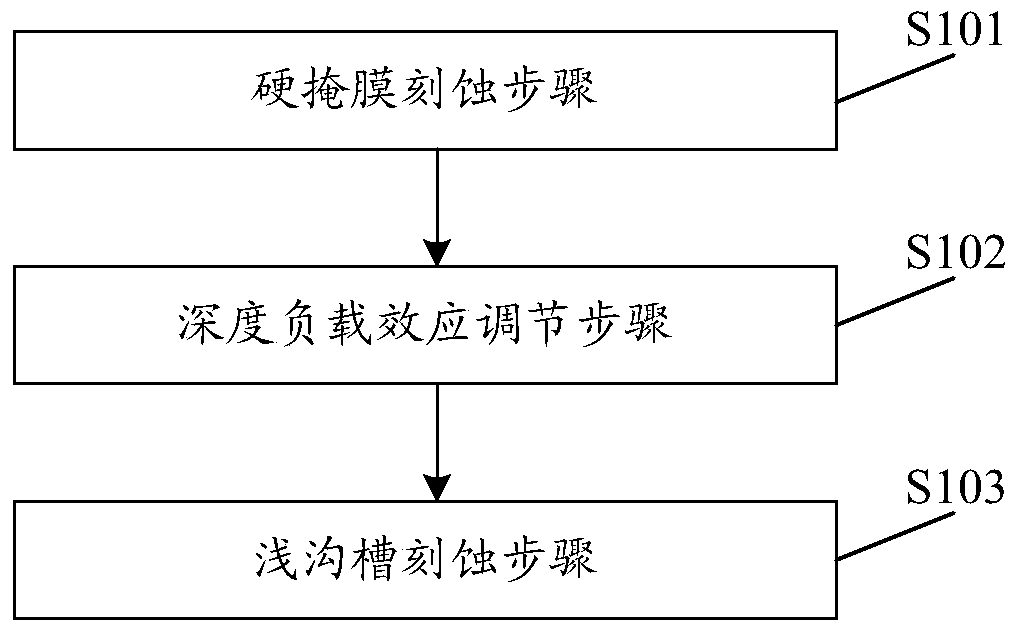
[0037] Specifically, such as figure 1 As shown, the etching method includes:

[0038] Step S101 , a hard mask etching step.

[0039] In the hard mask etching step, the hard mask at the large opening and the small opening are etched until the hard mask at th...


PUM


Abstract

The invention discloses a depth-load-adjustable etching method, relates to the technical field of a semiconductor, and can adjust the depth load effect of a silicon wafer under the premise of not increasing process. The depth-load-adjustable etching method comprises a hard mask etching step, a depth load effect adjusting step and a shallow trench etching step, and is characterized by, in the hard mask etching step, carrying out etching on a hard mask at the place of a big opening and at the place of a small opening until the hard mask at the big opening is removed completely, and a part of the hard mask at the place of the small opening is residual; in the depth load effect adjusting step, carrying out etching on the hard mask at the place of the small opening until the hard mask at the place of the small opening is removed completely, and etching the silicon at the place of the big opening, difference of the etching depth of the big opening and the etching depth of the small opening being adjustable; and in the shallow trench etching step, carrying out etching on the silicon at the place of the big opening and the place of the small opening.

Description

technical field [0001] The invention relates to the technical field of semiconductors, in particular to an etching method with adjustable depth load. Background technique [0002] In the actual production process, different types of etching machines are often required to perform trench etching of the same process on silicon wafers to produce the same type of products, but the depth loading effects of products produced by different types of etching machines are different, and thus There are also differences in electrical properties. Therefore, in order to meet the consistency of electrical properties of the same product, the depth loading effect of the same product produced by different types of etching machines needs to be consistent. [0003] The etching method in the prior art includes a hard mask main etching step, a hard mask over etching step and a shallow trench etching step, the depth loading effect mainly comes from the shallow trench etching step, and the hard mask ...

Claims


Application Information

Patent Timeline
Patent Type & Authority Patents(China)
IPC IPC(8): H01L21/311
CPCH01L21/31138
Inventor 符雅丽
Owner BEIJING NAURA MICROELECTRONICS EQUIP CO LTD
Why Eureka
Try Eureka