Check patentability & draft patents in minutes with Patsnap Eureka AI!

Array substrate and liquid crystal display device

An array substrate and black matrix technology, applied in the field of liquid crystal displays, can solve problems such as light leakage, phase change of polarized light, and easy disordered rotation of liquid crystals, etc., and achieve the effect of solving pixel light leakage

Active Publication Date: 2020-07-28
TCL CHINA STAR OPTOELECTRONICS TECH CO LTD
View PDF5 Cites 0 Cited by
  • Summary
  • Abstract
  • Description
  • Claims
  • Application Information

AI Technical Summary

Problems solved by technology

but for figure 1 The area indicated by the middle box 10—the area where the light-shielding transparent electrode 13 is adjacent to the black matrix 16 instead of overlapping up and down, because this area is close to the gate electrode of the TFT, at the end of the pixel electrode 15 and the light-shielding metal 14, the electric field is relatively disordered, and the liquid crystal Easy to rotate disorderly, resulting in phase change of polarized light, and no BM shielding, resulting in light leakage

Method used


Image

  • Array substrate and liquid crystal display device
  • Array substrate and liquid crystal display device
  • Array substrate and liquid crystal display device

Examples


Embodiment Construction

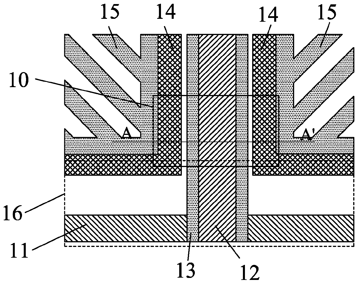
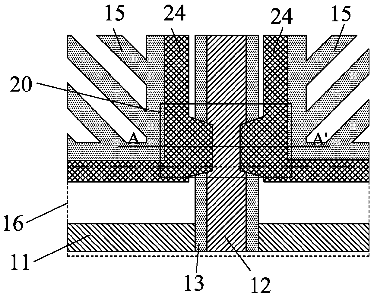
[0030] see image 3 , image 3 Viewed from the substrate side of the TFT array substrate, for the convenience of display and description, image 3 The substrate is omitted in , and the parts related to the DBS design in the array substrate structure are mainly shown, and the irrelevant parts will not be repeated here. Figure 4 for image 3 Schematic diagram of AA' section in middle, for the convenience of display and description, Figure 4 Enlarged and deformed, a substrate 17 is added. The array substrate of the present invention mainly includes: gate lines 11 and data lines 12, the gate lines 11 and the data lines 12 are intersected to define a plurality of pixel regions, and the pixel electrodes 15 are arranged in the pixel regions; The transparent electrode 13 is arranged up and down opposite to the data line 12, and the projection of the data line 12 on the light-shielding transparent electrode 13 falls into the light-shielding transparent electrode 13; the light-shi...


PUM


Abstract

The invention relates to an array substrate and a corresponding liquid crystal display device. The array substrate comprises a grid line, a data line, a shading transparent electrode and shading metaland is characterized in that the grid line and the data line are arranged in a crossed manner to define multiple pixel areas, and pixel electrodes are arranged in the pixel areas; the shading transparent electrode is vertically opposite to the data line, and projection of the data line on the shading transparent electrode falls into the shading transparent electrode; each shading metal is arranged along the edge of the corresponding pixel electrode; at least part of the data line and the shading metal vertically oppositely overlaps in an area, close a black matrix, of the shading transparentelectrode. By the array substrate and the liquid crystal display device, the pixel light leakage problem of the DBS technology is solved.

Description

technical field [0001] The invention relates to the field of liquid crystal displays, in particular to an array substrate and a liquid crystal display device. Background technique [0002] The HVA (High Vertical Alignment) mode is a relatively advanced one among the VA (Vertical Alignment) modes, and is used by many manufacturers in the LCD industry to produce large-size LCD screens. The traditional HVA mode uses BM (black matrix) to shade the gate (gate) and data (data) lines of the pixel. BM) expression, referred to as DBS. [0003] Existing liquid crystal display panels generally include a TFT (thin film transistor) array substrate, a CF (color filter) substrate disposed opposite to the TFT array substrate, and a liquid crystal layer disposed between the TFT array substrate and the CF substrate. figure 1 It is a schematic top view of the existing DBS-designed array substrate structure, viewed from the substrate side of the TFT array substrate, for the convenience of dis...

Claims


Application Information

Patent Timeline
Patent Type & Authority Patents(China)
IPC IPC(8): G02F1/1362G02F1/1343
Inventor 叶岩溪
Owner TCL CHINA STAR OPTOELECTRONICS TECH CO LTD
Features
  • R&D
  • Intellectual Property
  • Life Sciences
  • Materials
  • Tech Scout
  • Unparalleled Data Quality
  • Higher Quality Content
  • 60% Fewer Hallucinations
Learn More