Check patentability & draft patents in minutes with Patsnap Eureka AI!

Array substrate and preparation method thereof, and OLED display panel

A technology for array substrates and display panels, which is applied in the direction of electrical components, diodes, and electric solid-state devices. It can solve the problems of impurity in monochromatic light and affect the display, and achieve the effect of solving the problem of pixel light leakage and improving the display quality.

Inactive Publication Date: 2019-08-06
SHENZHEN CHINA STAR OPTOELECTRONICS SEMICON DISPLAY TECH CO LTD
View PDF5 Cites 7 Cited by
  • Summary
  • Abstract
  • Description
  • Claims
  • Application Information

AI Technical Summary

Problems solved by technology

[0003] The present invention provides an array substrate and its preparation method, and an OLED display panel to solve the technical problem of impure monochromatic light caused by pixel light leakage in the existing COA structure, thereby affecting the display

Method used


Image

  • Array substrate and preparation method thereof, and OLED display panel
  • Array substrate and preparation method thereof, and OLED display panel
  • Array substrate and preparation method thereof, and OLED display panel

Examples


Embodiment Construction

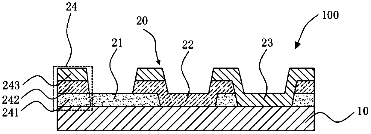
[0026] The following descriptions of the various embodiments refer to the accompanying drawings to illustrate specific embodiments in which the invention may be practiced. The directional terms mentioned in the present invention, such as [top], [bottom], [front], [back], [left], [right], [inside], [outside], [side], etc., are only for reference The orientation of the attached schema. Therefore, the directional terms used are used to illustrate and understand the present invention, but not to limit the present invention. In the figures, structurally similar elements are denoted by the same reference numerals.

[0027] The present invention is aimed at the technical problem that monochromatic light is impure due to pixel light leakage in the COA structure array substrate of the existing OLED display panel, which further affects the display. This embodiment can solve this defect.

[0028] Such as figure 1 As shown, this embodiment provides an array substrate 100 , including a ...


PUM


Abstract

An array substrate comprises a thin film transistor array substrate and a color filter layer. The color filter layer comprises a first color resistance layer, a second color resistance layer, a thirdcolor resistance layer, and a composite color resistance shading layer separating the first color resistance layer, the second color resistance layer and the third color resistance layer. The composite color resistance shading layer comprises a first sub-film, a second sub-film and a third sub-film stacked in turn. Under the condition of not adding a mask process, the problem of pixel light leakage can be solved by changing the color film structure in the COA structure, and thus, the display quality of the panel can be improved.

Description

technical field [0001] The invention relates to the field of display technology, in particular to an array substrate, a preparation method thereof, and an OLED display panel. Background technique [0002] OLED (Organic Light-Emitting Diode, organic electroluminescent diode) devices are widely used in the display field because of their advantages such as self-luminescence, wide viewing angle, high contrast, low power consumption, and high response rate. With the development of curved display panels, it is also gradually developing towards large-size panels. Due to the IR drop (voltage drop) problem in the display panel of the top emission structure, the bottom emission structure is the preferred structure in the large-size panel. However, the COA (Color Filter On Array, color filter is prepared on the array substrate) structure of the bottom emission OLED display panel has the problem of pixel light leakage, which leads to the impurity of single light, which further affects ...

Claims


Application Information

Patent Timeline
IPC IPC(8): H01L27/32
CPCH10K59/38H10K59/12H10K59/1201
Inventor 范英春
Owner SHENZHEN CHINA STAR OPTOELECTRONICS SEMICON DISPLAY TECH CO LTD
Features
  • R&D
  • Intellectual Property
  • Life Sciences
  • Materials
  • Tech Scout
  • Unparalleled Data Quality
  • Higher Quality Content
  • 60% Fewer Hallucinations
Learn More