

Semiconductor device and method for manufacturing the same
a semiconductor device and manufacturing method technology, applied in the direction of semiconductor devices, basic electric elements, electrical equipment, etc., can solve the problems of unstable operation of semiconductor devices, significant reduction of yield, etc., and achieve favorable display, favorable electric characteristics, and increase the area of a pixel portion
- Summary
- Abstract
- Description
- Claims
- Application Information
AI Technical Summary
Benefits of technology
Problems solved by technology
Method used
Image

Examples
embodiment 1
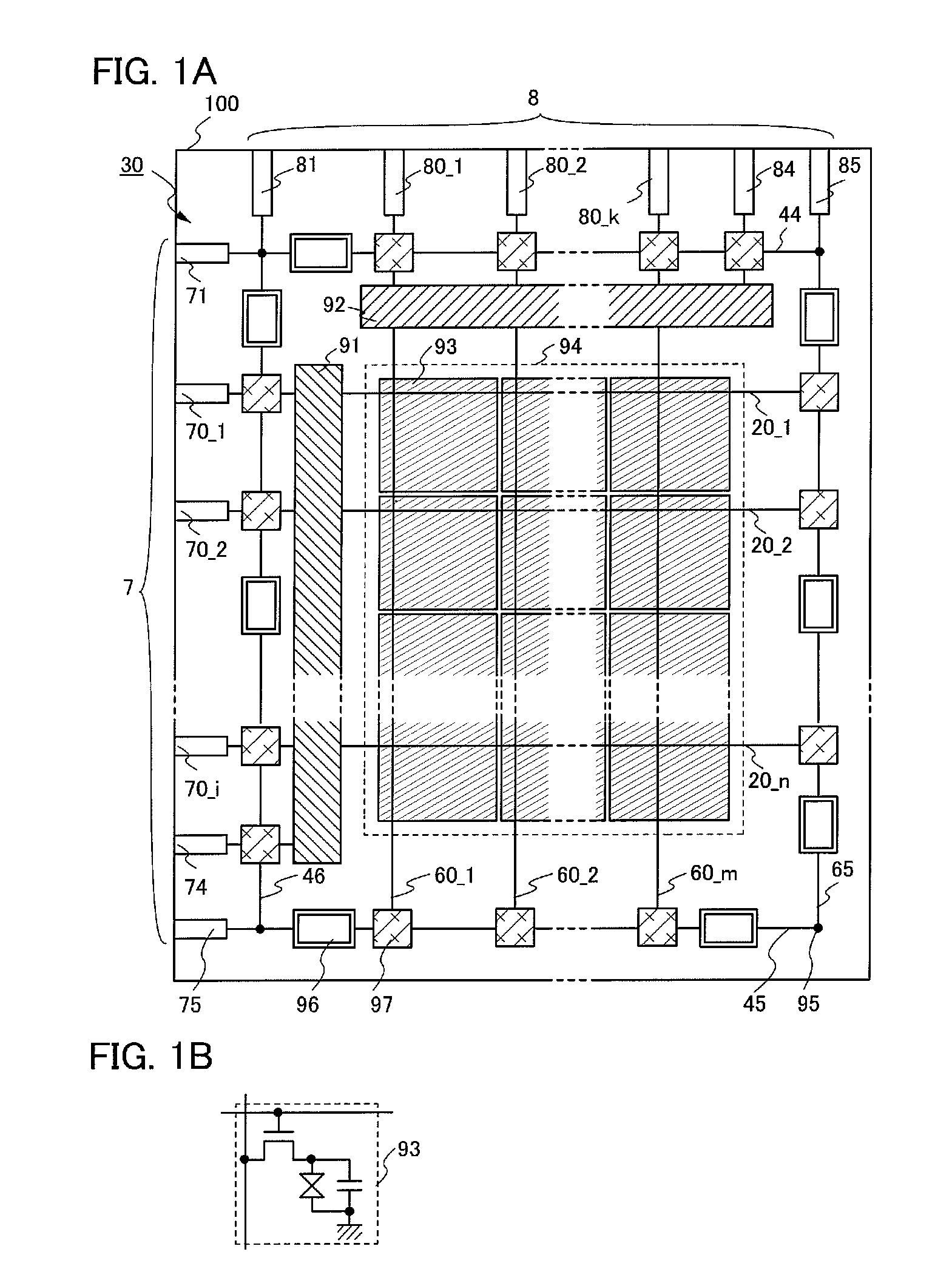
[0084]In this embodiment, one embodiment of a display device where semiconductor elements that include an oxide semiconductor and are provided in the pixel and the periphery of the pixel portion are formed will be described with reference to FIGS. 1A and 1B.
[0085]FIG. 1A illustrates a structure of a display device 30. The display device 30 includes a gate terminal portion 7 and a source terminal portion 8 over a substrate 100. The display device 30 is provided with gate wirings (20_1 to 20—n (note that n is a natural number)) including the gate wiring 20_1 and the gate wiring 20_2, and source wirings (60_1 to 60—m (note that m is a natural number)) including the source wiring 60_1 and the source wiring 60_2. Further, in a pixel region 94 of the display device 30, pixels 93 are arranged in matrix. Note that each of the pixels 93 is connected to at least one gate wiring and one source wiring.
[0086]Further, the display device 30 includes a common wiring 44, a common wiring 45, a common...
embodiment 2
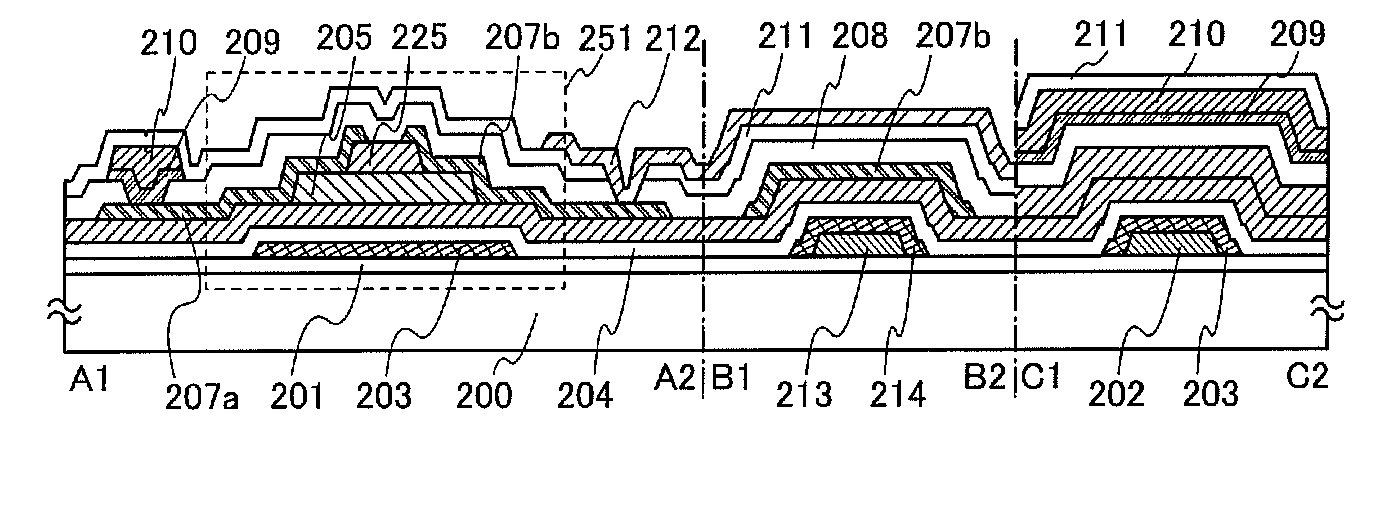
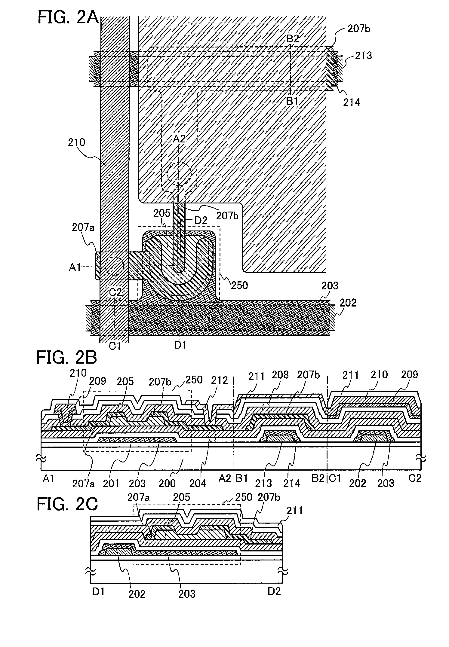
[0106]In this embodiment, a manufacturing process of a pixel portion in the display device described in Embodiment 1 will be described with reference to FIGS. 4A to 4D and FIGS. 5A to 5C. Note that cross section A1-A2, cross section B1-B2, cross section C1-C2, and cross section D1-D2 in FIGS. 4A to 4D and FIGS. 5A to 5C are cross-sectional views taken along chain lines A1-A2, B1-B2, C1-C2, and D1-D2 in FIG. 2A, respectively.
[0107]First, as a base insulating layer, the insulating layer 201 including silicon nitride is formed to a thickness of greater than or equal to 50 nm and less than or equal to 300 nm, preferably greater than or equal to 100 nm and less than or equal to 200 nm, over the substrate 200. As the substrate 200, in addition to a glass substrate and a ceramic substrate, a plastic substrate or the like with heat resistance to withstand a process temperature in this manufacturing process can be used. In the case where the substrate does not need a light-transmitting prope...
embodiment 3
[0221]In this embodiment, an example of a structure of a thin film transistor used for the gate driver circuit 91 or the source driver circuit 92 of the display device 30 which is described in Embodiment 1 with reference to FIGS. 1A and 1B will be described.
[0222]A driver circuit for driving a pixel portion is formed using an inverter circuit, a capacitor, a resistor, and the like. In this embodiment, a structure of an inverter circuit which includes two thin film transistors as thin film transistors used in the driver circuit is described. When the inverter circuit is formed using two n-channel TFTs in combination, there are an inverter circuit having two enhancement type TFTs (hereinafter referred to as an EEMOS circuit) and an inverter circuit having a combination of an enhancement type transistor and a depletion type transistor (hereinafter referred to as an EDMOS circuit). Note that an n-channel TFT whose threshold voltage is positive is referred to as an enhancement type trans...
PUM
| Property | Measurement | Unit |
|---|---|---|
| size | aaaaa | aaaaa |
| temperature | aaaaa | aaaaa |
| temperature | aaaaa | aaaaa |
Abstract
Description
Claims
Application Information