
A method for detecting mura defects of amoled display

A defect detection and display technology, applied in image analysis, image enhancement, instruments, etc., can solve the problems of uneven display area, uneven brightness display of screen area, unclear edge outline, etc. average image effect

Active Publication Date: 2021-07-02
HARBIN INST OF TECH SHENZHEN GRADUATE SCHOOL
View PDF2 Cites 0 Cited by
  • Summary
  • Abstract
  • Description
  • Claims
  • Application Information

AI Technical Summary

Problems solved by technology

Because there are various defects in the manufacturing process of AMOLED display screens, such as point defects, line defects, and Mura defects (the name of Mura comes from a Japanese word, specifically referring to panel defects, which is used to represent when the display is displayed at a constant brightness. , the unevenness of the display area) will have an impact on the uniformity of light emission, image clarity, and life of the AMOLED display.
[0003] Mura defect is a bad defect that seriously affects the picture quality of AMOLED display, mainly manifested as uneven brightness display in the screen area
There are many types and shapes of mura defects, and the contrast is low, the position is not fixed, and the edge outline is not clear. Compared with other optical defects of the display, mura defects are more difficult to detect
The traditional human eye detection method mainly relies on the experience and subjective feelings of the inspector to detect mura defects and evaluate their grades, which may lead to inconsistent judgment results of different inspectors for the same mura defect

Method used


Image

  • A method for detecting mura defects of amoled display
  • A method for detecting mura defects of amoled display
  • A method for detecting mura defects of amoled display

Examples


Embodiment Construction

[0015] The present invention will be further described below in conjunction with the description of the drawings and specific embodiments.

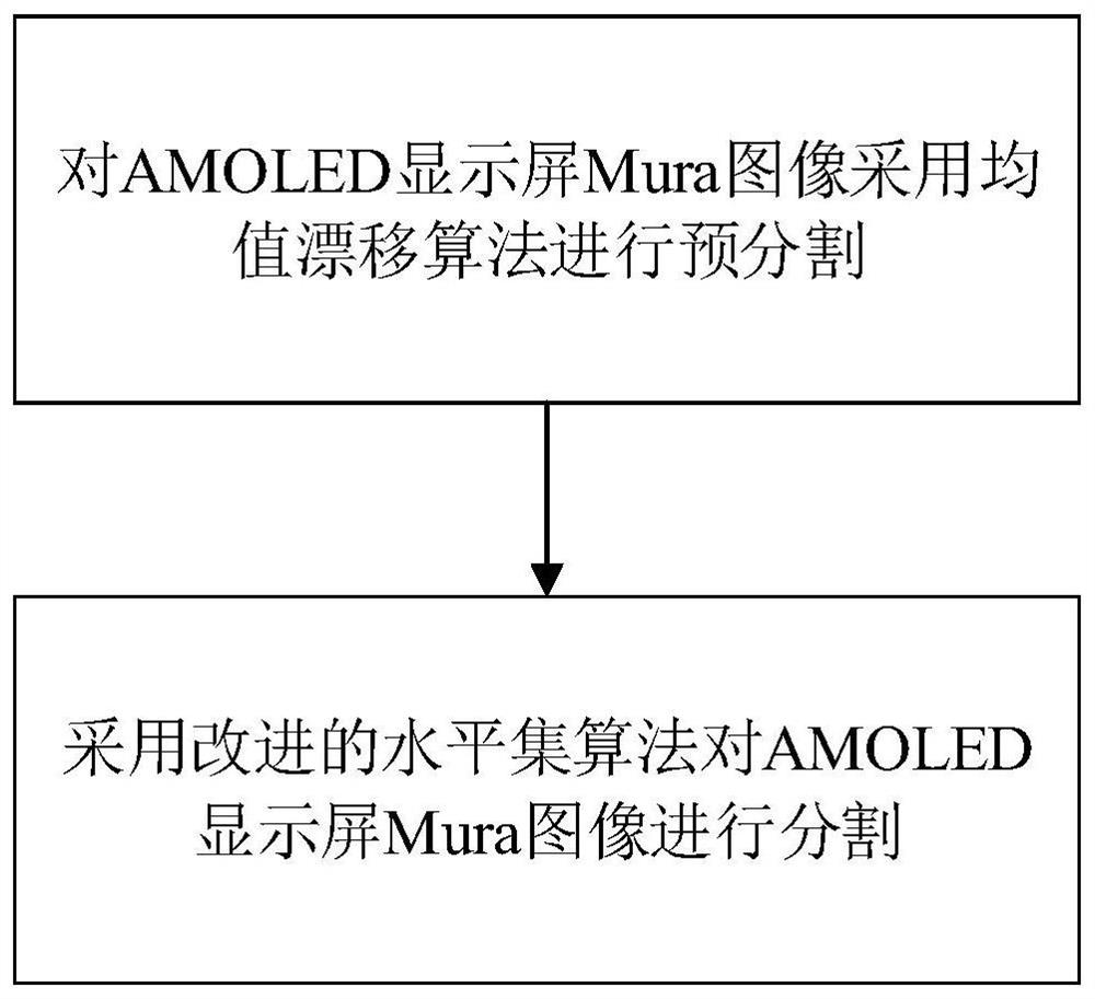
[0016] Such as Figure 1 to Figure 4 Shown, a kind of AMOLED display screen Mura defect detection method comprises:

[0017] 1. Use the mean shift algorithm to pre-segment the Mura image of the AMOLED display;

[0018] 2. Using the improved level set algorithm to segment the Mura image of AMOLED display screen.

[0019] The first unit, the mean shift algorithm, has an iterative process. First calculate the mean shift value of the current point, then move the point to the mean shift value, and then use this as a new starting point to continue moving until certain conditions are met. Its derivation process is as follows:

[0020] Assuming a d-dimensional space R d There are n sample points, use x i Indicates the attribute value of each sample point, where i=1,2,...,n. in R d Choose a sample point x in , and the mean shift vector of p...


PUM


Abstract

The invention provides a Mura defect detection method of an AMOLED display screen. Firstly, a mean shift algorithm is used to pre-segment the Mura image of an AMOLED display screen to obtain the initial contour required by the level set algorithm, and then the local and global information combined with the image is used. The level set algorithm of the AMOLED display Mura image is segmented. The beneficial effect of the invention is that the problem that the local image model is sensitive to the initial contour is solved, and the proposed level set algorithm combines the local and global information of the image to solve the problem that the global image model cannot process images with uneven gray levels.

Description

technical field [0001] The invention relates to a method for detecting a display screen, in particular to a method for detecting a Mura defect of an AMOLED display screen. Background technique [0002] Active Matrix Organic Light Emitting Diode Panel (AMOLED) is regarded as the next generation display technology, which has the characteristics of fast response, high contrast, wide viewing angle and low energy consumption. Because there are various defects in the manufacturing process of AMOLED display screens, such as point defects, line defects, and Mura defects (the name of Mura comes from a Japanese word, specifically referring to panel defects, which is used to represent when the display is displayed at a constant brightness. , the non-uniformity of the display area) will have an impact on the uniformity of light emission, image clarity, and life of the AMOLED display. [0003] Mura defect is a bad defect that seriously affects the picture quality of AMOLED display, main...

Claims


Application Information

Patent Timeline
Patent Type & Authority Patents(China)
IPC IPC(8): G06T7/00G06T7/13G06T7/143G06T7/12G06T7/149
CPCG06T7/0004G06T2207/20076G06T2207/20116G06T2207/30108G06T7/12G06T7/13G06T7/143G06T7/149
Inventor 肖君军李雄杰姚杏枝
Owner HARBIN INST OF TECH SHENZHEN GRADUATE SCHOOL
Learn More