Electromagnetic shielding packaging method of point pre-fixed thin film circuit
A thin-film circuit and electromagnetic shielding technology, which is applied in the direction of circuit devices, circuits, printed circuits, etc., can solve problems such as difficult to avoid circuit electromagnetic interference, inconvenient metal cavity processing, etc.
- Summary
- Abstract
- Description
- Claims
- Application Information
AI Technical Summary
Problems solved by technology
Method used
Image

Examples
Embodiment approach
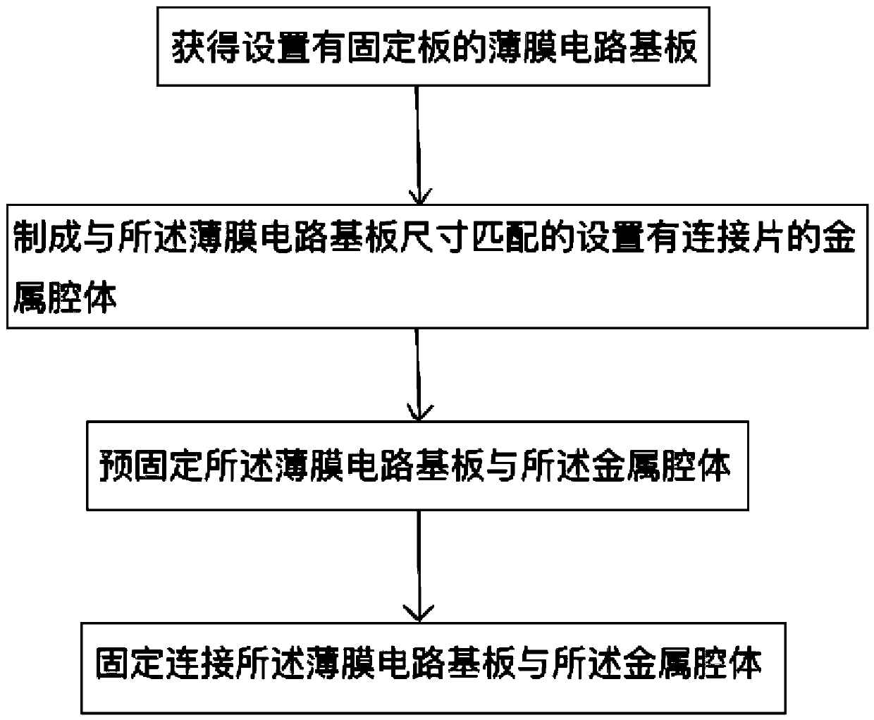
[0020] An electromagnetic shielding packaging method for point pre-fixed film circuits, comprising:
[0021] Step (a) obtaining a thin film circuit substrate provided with a fixing plate;
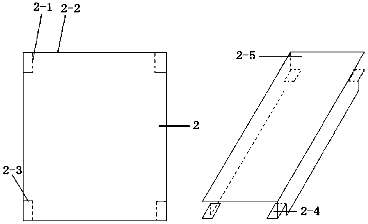
[0022] Step (b) making a metal cavity provided with connecting pieces matching the size of the thin film circuit substrate;
[0023] Step (c) pre-fixing the thin film circuit substrate and the metal cavity.
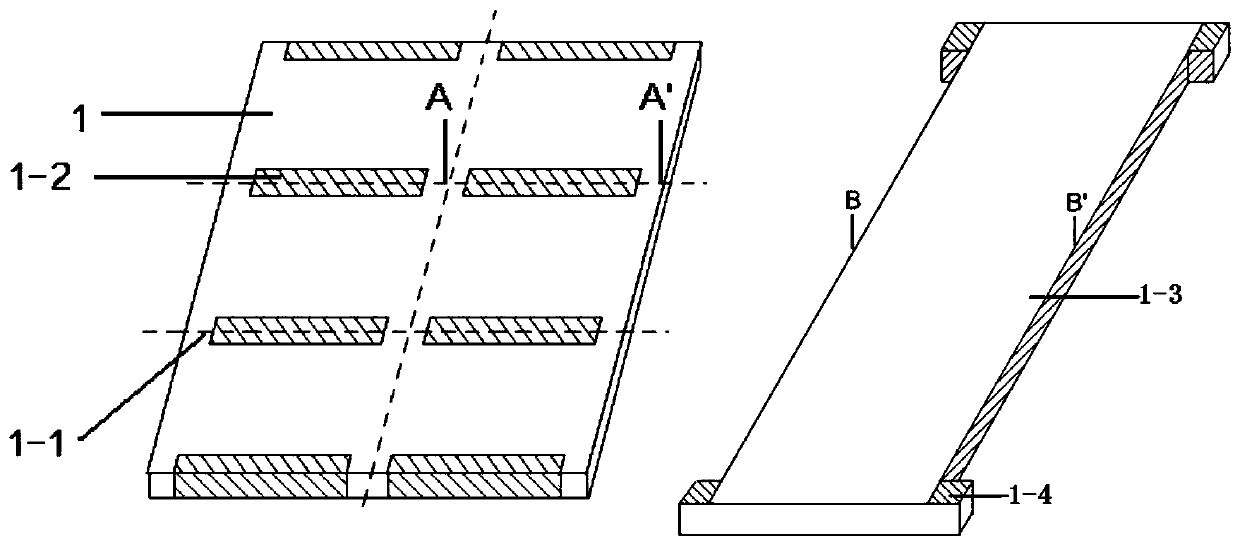
[0024] Further, the front side surface of the thin film circuit substrate is covered with a metal film. The front and side of the thin film circuit substrate are covered with a metal film, which can effectively guarantee the metal interconnection effect on the side of the circuit.
[0025] Further, the method for obtaining a thin film circuit substrate provided with a fixing plate includes:
[0026] Step (a-1) opening an array through cavity shorter than the length of the circuit along the circuit array in the circuit substrate;
[0027] Step (a-2) plating a metal film on the surfa...
PUM
 Abstract
Description
Claims
Application Information
PatSnap Eureka turns technology decisions into work you can execute. Powered by our Innovation Knowledge Graph, it runs expert workflows across engineering, life sciences, materials and intellectual property. Get your review-ready output in minutes.


