

Housing assembly, antenna assembly and electronic device
A technology of housing assembly and antenna assembly, applied in the field of electronics, can solve the problems of limited space of electronic equipment, increase the size of electronic equipment, etc., to achieve the effect of improving the intensity of radiated signals and increasing the clearance area
- Summary
- Abstract
- Description
- Claims
- Application Information
AI Technical Summary
Problems solved by technology
Method used
Image

Examples
Embodiment Construction
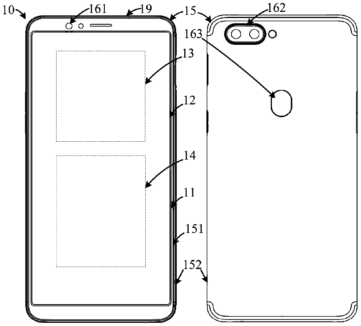
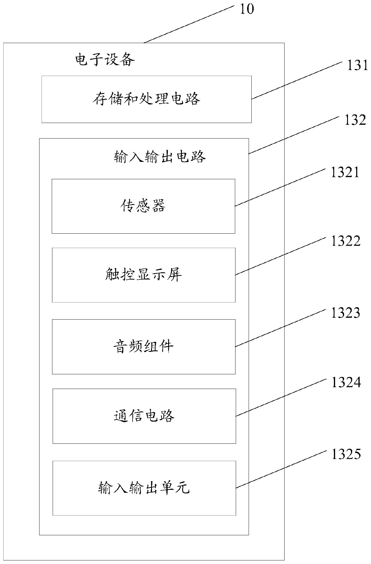
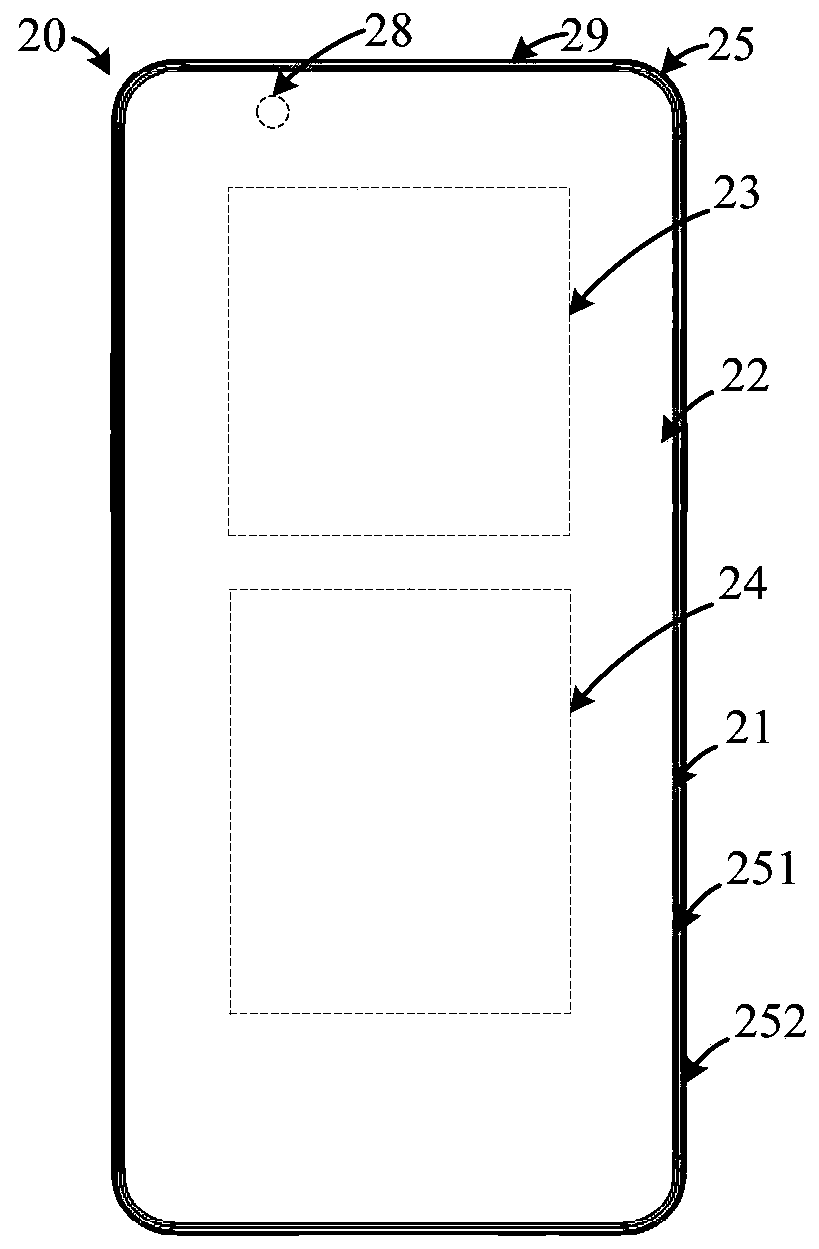
[0046] The technical solutions in the embodiments of the present application will be clearly and completely described below with reference to the accompanying drawings in the embodiments of the present application. Obviously, the described embodiments are only a part of the embodiments of the present application, but not all of the embodiments. Based on the embodiments in the present application, all other embodiments obtained by those skilled in the art without creative work fall within the protection scope of the present application.
[0047] In the description of this application, it should be understood that the terms "center", "longitudinal", "lateral", "length", "width", "thickness", "upper", "lower", "front", " rear, left, right, vertical, horizontal, top, bottom, inside, outside, clockwise, counterclockwise, etc., or The positional relationship is based on the orientation or positional relationship shown in the accompanying drawings, which is only for the convenience ...
PUM
 Abstract
Description
Claims
Application Information