Display device and pixel circuit thereof, and driving method

A technology of pixel circuits and row pixels, applied in static indicators, instruments, etc., can solve the problems of uneven distribution of threshold voltage and mobility, etc., and achieve the effects of small data input voltage range, good display contrast, and simple control signals

Active Publication Date: 2018-12-07
PEKING UNIV SHENZHEN GRADUATE SCHOOL
View PDF9 Cites 5 Cited by
  • Summary
  • Abstract
  • Description
  • Claims
  • Application Information

AI Technical Summary

Problems solved by technology

[0004] The present application provides a display device and its pixel circuit and driving method to solve the problem of uneven distribution of threshold voltage and mobility in the prior art

Method used


Image

  • Display device and pixel circuit thereof, and driving method
  • Display device and pixel circuit thereof, and driving method
  • Display device and pixel circuit thereof, and driving method

Examples


Embodiment 1

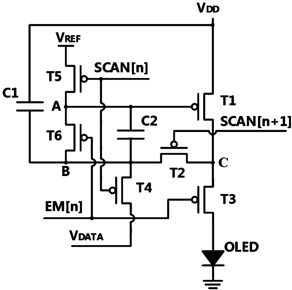
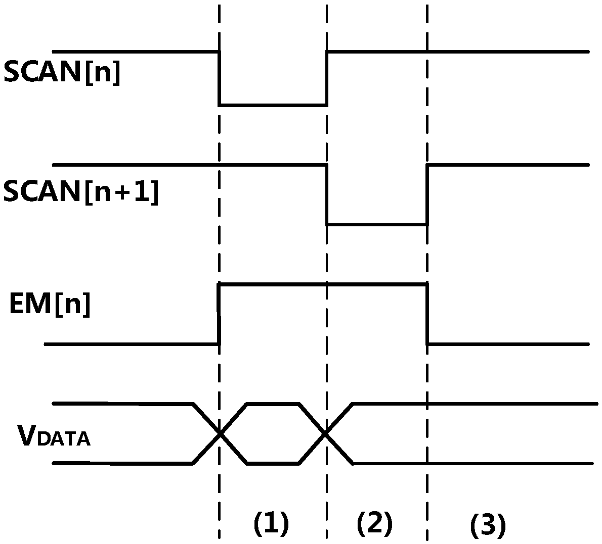
[0058] Please refer to figure 1 , is a structure diagram of a pixel circuit disclosed in Embodiment 1, including: DD and the drive transistor T1 and the third transistor T3 between the light emitting element OLED, the second transistor T2, the fourth transistor T4, the fifth transistor T5, the sixth transistor T6 and the capacitor C1 and the capacitor C2. also includes the power line V DD , data line V DATA , reference voltage line V REF , scan line SCAN[n], scan line SCAN[n+1] and luminous control signal line EM[n], where n represents the row number of the pixel circuit, such as scan line SCAN[n], scan line SCAN[n +1] represent the scanning lines of the nth row of pixel circuits and the scanning lines of the n+1th row of pixel circuits. Similarly, the emission control signal line EM[n] represents the emission control signal line of the nth row of pixel circuits. Wherein, the scan line of the row where the pixel circuit disclosed in this embodiment is called the scan line ...

Embodiment 2

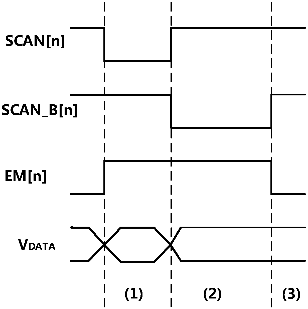
[0079] Figure 5 It is a structural diagram of a pixel circuit disclosed in the second embodiment. Figure 5 The circuit structure and figure 1 The circuit structure is similar, including: for series connection on the power line V DD and the drive transistor T1 and transistor T3 between the light emitting element OLED, and the second transistor T2, the fourth transistor T4, the fifth transistor T5, the sixth transistor T6 and the capacitor C1 and the capacitor C2. also includes the power line V DD , data line V DATA , reference voltage line V REF , scanning line SCAN[n], scanning line SCAN[n+1] and light emitting control signal line EM[n]. Wherein, the scan line of the row where the pixel circuit disclosed in this embodiment is called the scan line SCAN[n] of the row. The scan line next to the row where the pixel circuit is located is referred to as the next scan line SCAN[n+1]. The power supply line of the pixel circuit V DD Used to provide power to the pixel circuit....

Embodiment 3

[0089] Figure 6 It is a structure diagram of a pixel circuit disclosed in Embodiment 3, Figure 6 The circuit structure and figure 1 The circuit structure is similar, the difference is that Figure 6 The upper plate of the first capacitor C1 in the shown pixel circuit is connected to the reference potential line V REF , instead of figure 1 The upper plate of the first capacitor C1 in the shown pixel circuit is connected to the power line V DD . In this embodiment, the first capacitor C1 is connected to the reference potential V REF able to reduce the power line V DD capacitive load, reducing the dynamic power consumption of the display. Also, due to the relative V DD For example, the reference potential line V REF The upper voltage is more stable, connect the second capacitor C2 to the reference potential line V REF It can ensure that the output voltage of the upper and lower plates of the capacitor module is more stable. Figure 6 The driving timing diagram of the...


PUM


Abstract

The invention discloses a display device and a pixel circuit thereof, and a driving method. The pixel circuit of the invention includes a driving transistor, second to fifth transistors and a second capacitor. The driving transistor is used for providing a driving current for a light emitting device. The second to fifth transistors are used as switching tubes, and are used for responding to scanning signals, data signals and light emitting control signals. The second capacitor is used for storing sampling voltages. Compensation is made for the threshold voltage of the driving transistor in order to reduce the influence of non-uniform mobility of the transistors and improve the contrast of the display device. The display device supports a progressive light emission mode and a simultaneous light emission mode, and can be applied in a high-resolution or high-frame-frequency display device.

Description

technical field [0001] The present invention relates to the field of display technology, in particular to a display device, a pixel circuit and a driving method thereof. Background technique [0002] Organic Light-Emitting Diode (OLED) display has been extensively studied in recent years due to its advantages of high brightness, high luminous efficiency, wide viewing angle and low power consumption, and has been rapidly applied to a new generation of display devices. [0003] The OLED display can be driven in two ways: passive matrix OLED (PMOLED) and active matrix OLED (AMOLED). Although the cost of passive matrix driving is low, it cannot realize high-resolution display due to crosstalk phenomenon, and the passive matrix driving current is large, which reduces the service life of OLED. In contrast, the active matrix driving method sets a different number of transistors on each pixel as a current source, which avoids crosstalk, requires less driving current, and lower powe...

Claims


Application Information

Patent Timeline
Patent Type & Authority Applications(China)
IPC IPC(8): G09G3/3258G09G3/3266G09G3/3291
CPCG09G3/3258G09G3/3266G09G3/3291
Inventor 张盛东吴继祥廖聪维王莹霍新新易水平谢锐彬
Owner PEKING UNIV SHENZHEN GRADUATE SCHOOL
Why Eureka
Try Eureka