Method for manufacturing double-sided circuit substrate and double-sided circuit substrate

A technology of circuit substrate and manufacturing method, which is applied in the direction of printed circuit manufacturing, circuit, printed circuit, etc., can solve the problems such as unable to present images, and achieve the effect of avoiding electrical connection failure and avoiding the increase of shading area

Active Publication Date: 2019-07-02
AU OPTRONICS CORP
View PDF7 Cites 0 Cited by
  • Summary
  • Abstract
  • Description
  • Claims
  • Application Information

AI Technical Summary

Problems solved by technology

The display area of ​​the display panel can present images, while the edge area is a dark area that cannot present images

Method used


Image

  • Method for manufacturing double-sided circuit substrate and double-sided circuit substrate
  • Method for manufacturing double-sided circuit substrate and double-sided circuit substrate
  • Method for manufacturing double-sided circuit substrate and double-sided circuit substrate

Examples


Embodiment Construction

[0067] Below in conjunction with accompanying drawing, structural principle and working principle of the present invention are specifically described:

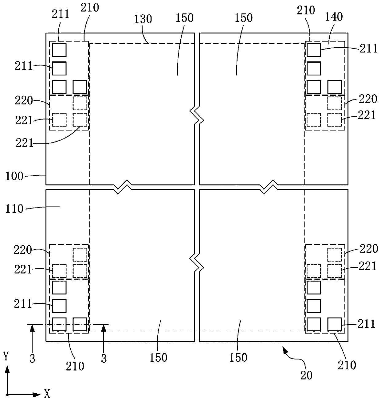
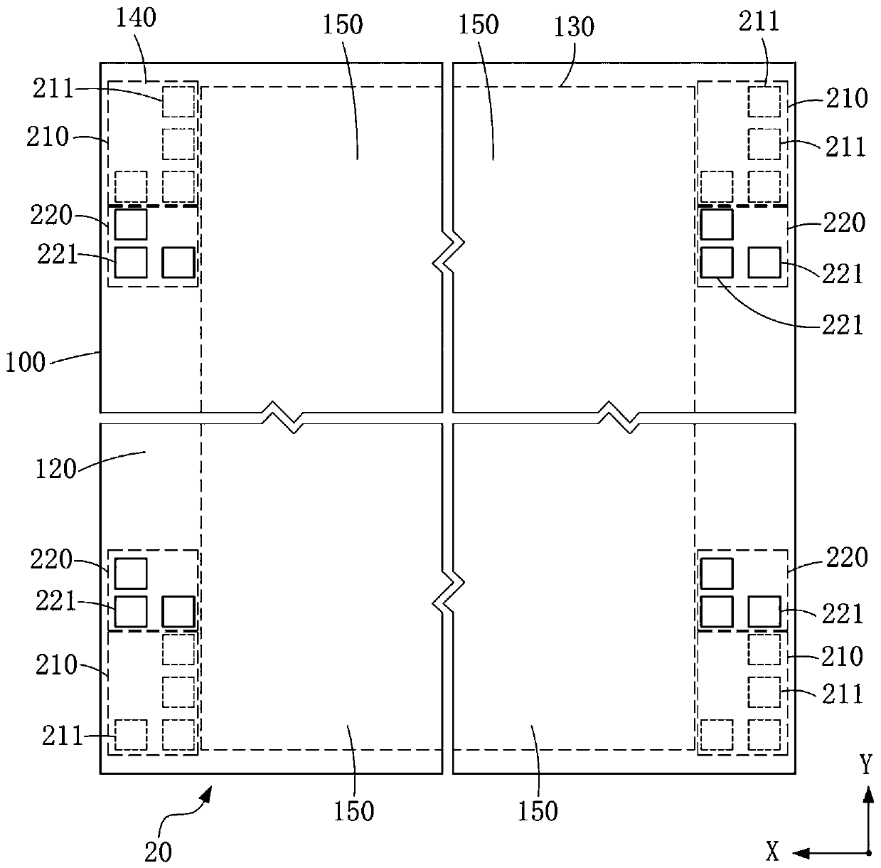
[0068] Please refer tofigure 1 and figure 2 , figure 1 Shown is a schematic top view of a double-sided circuit substrate 20 according to an embodiment of the present invention, figure 2 shown as figure 1 A schematic bottom view of the double-sided circuit substrate 20 of FIG. In this embodiment, the double-sided circuit substrate 20 is used to make a display panel, but it is not limited thereto. The double-sided circuit substrate 20 includes a substrate 100 , a first alignment mark 210 and a second alignment mark 220 . The substrate 100 includes a first surface 110 and a second surface 120 , and the first surface 110 and the second surface 120 are opposite to each other. The first alignment mark 210 is located on the first surface 110 , and the second alignment mark 220 is located on the second surface 120 . In this em...


PUM


Abstract

The invention relates to a method for manufacturing a double-sided circuit substrate and a double-sided circuit substrate. The manufacturing method comprises the steps of providing a substrate, wherein the substrate comprises a first surface and a second surface, and the first surface and the second surface are opposite to each other; forming a first alignment mark and a first patterned circuit onthe first surface; sensing the position of the first alignment mark by using an optical positioning device; forming a second alignment mark on the second surface according to the position of the first alignment mark; sensing the position of the second alignment mark by using an optical positioning device; and forming a second patterned circuit on the second surface according to the position of the second alignment mark, wherein the second patterned circuit is aligned with the first patterned circuit in the normal direction of the substrate.

Description

technical field [0001] The invention relates to a method for manufacturing a circuit substrate, and in particular to a method for manufacturing a double-sided circuit substrate and the double-sided circuit substrate. Background technique [0002] The existing display device includes a display panel, the display panel includes a substrate, a plurality of pixel units and a plurality of edge elements, the substrate includes a display area and an edge area surrounding the display area, the pixel units are arranged in the display area, and the edge elements are arranged In the edge area, the edge element is further connected to the corresponding pixel unit, and the edge element can be used to drive the pixel unit or also be used as a ground circuit of the pixel unit. The display area of ​​the display panel can present images, while the edge area is a dark area and cannot present images. Therefore, the display device has a frame to cover the edge area and only expose the display ...

Claims


Application Information

Patent Timeline
Patent Type & Authority Applications(China)
IPC IPC(8): H05K1/02H05K3/02H01L23/492
CPCH01L23/492H05K1/0269H05K3/02
Inventor 吕明潔张毓宽
Owner AU OPTRONICS CORP
Why Eureka
Try Eureka