Display panel and production method thereof

A display panel and manufacturing method technology, applied in the direction of electrical components, electrical solid devices, circuits, etc., can solve the problems of low yield rate, difficulty in mass production, and difficulty in silicon-based micro-display panels, so as to improve resolution, The effect of reducing the occupied area

Active Publication Date: 2019-11-15
CHENGDU VISTAR OPTEOLECTRONICS CO LTD
View PDF6 Cites 7 Cited by
  • Summary
  • Abstract
  • Description
  • Claims
  • Application Information

AI Technical Summary

Problems solved by technology

[0003] However, the existing colorization of silicon-based micro-display panels has pr

Method used


Image

  • Display panel and production method thereof
  • Display panel and production method thereof
  • Display panel and production method thereof

Examples


Embodiment Construction

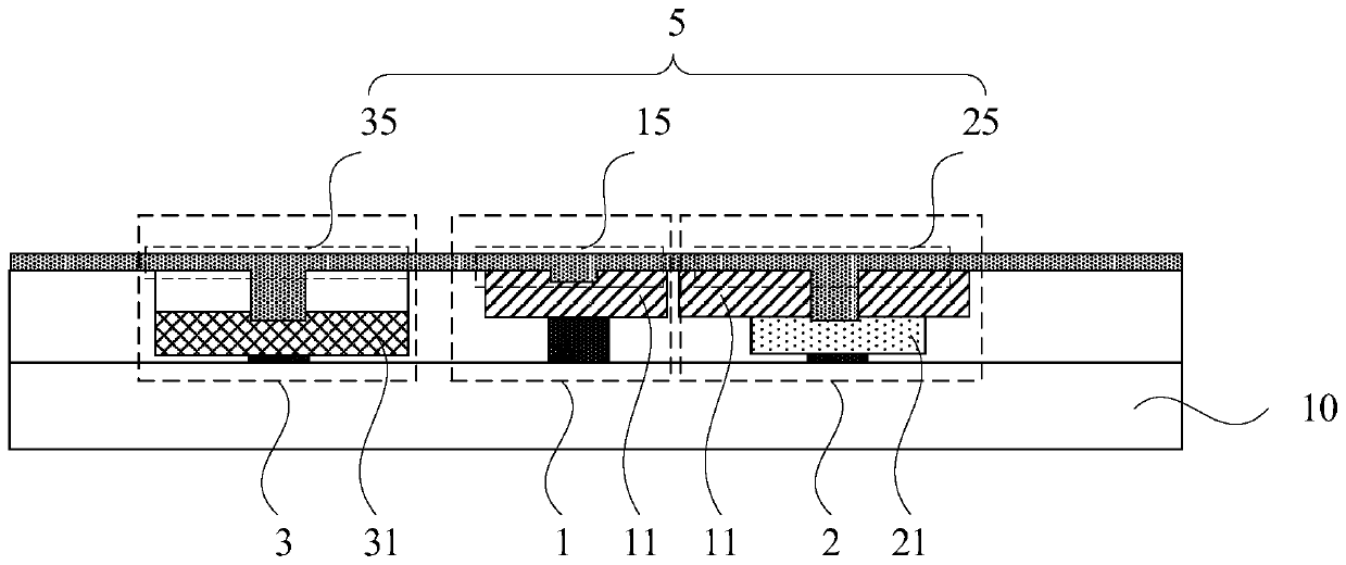
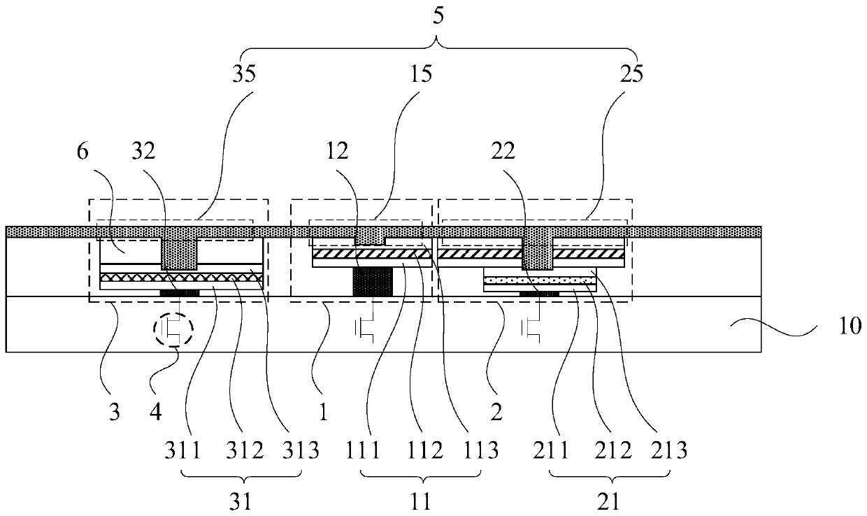
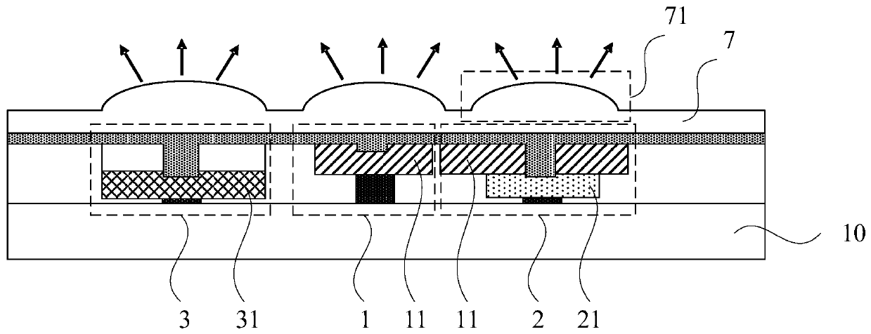
[0041] The present invention will be further described in detail below in conjunction with the accompanying drawings and embodiments. It should be understood that the specific embodiments described here are only used to explain the present invention, but not to limit the present invention. In addition, it should be noted that, for the convenience of description, only some structures related to the present invention are shown in the drawings but not all structures.

[0042] figure 1 It is a schematic structural diagram of a display panel provided by an embodiment of the present invention. see figure 1 , the display panel includes a backplane 10 and a plurality of first light-emitting devices 1, a plurality of second light-emitting devices 2 and a plurality of third light-emitting devices 3 on the backplane 10, the first light-emitting devices 1, the second light-emitting devices 2 It is different from the light emitting color of the third light emitting device 3 . And along...


PUM


Abstract

The embodiment of the invention discloses a display panel and a production method thereof. The display panel includes a backplane, and a plurality of first light emitting devices, a plurality of second light emitting devices and a plurality of third light emitting devices on the backplane. The first light emitting devices, the second light emitting devices and the third light emitting devices emitlight of different colors. The second light emitting devices overlap with the first light emitting devices in a direction perpendicular to the display panel. Through the technical scheme of the invention, color display of the display panel is realized with lower process difficulty, fewer process steps and higher production yield under the condition that the sizes of the light emitting devices ofthe display panel are very small.

Description

technical field [0001] Embodiments of the present invention relate to the field of display technology, and in particular to a display panel and a manufacturing method thereof. Background technique [0002] Silicon-based microdisplay technology is about combining display with monocrystalline silicon integrated circuits. The display panel using silicon-based microdisplay technology has the advantages of high display resolution, large viewing angle, fast response speed, high brightness and low power consumption, which makes silicon Silicon-based microdisplay technology has broad application prospects in increasing image display size and definition, reducing the number of system chips to reduce system cost and product space volume. At present, silicon-based microdisplay technology can be used in military, medical, aerospace and Consumer electronics and other fields. [0003] However, the existing colorization of silicon-based micro-display panels has the problems of great diffi...

Claims


Application Information

Patent Timeline
IPC IPC(8): H01L27/15H01L33/00H01L33/38H01L33/48
CPCH01L27/156H01L33/48H01L33/0075H01L33/38H01L2933/0033
Inventor 田文亚郭恩卿王程功
Owner CHENGDU VISTAR OPTEOLECTRONICS CO LTD
Why Eureka
Try Eureka