A kind of oled panel, the preparation method of oled panel and display device

A panel and substrate technology, applied in the field of OLED panel, OLED panel preparation method and display device, can solve the problems of low blue light luminous efficiency, poor blue light transmittance, reduced blue light transmittance, etc., so as to increase the light transmittance, improve the Transmittance, the effect of reducing the loss of light transmission

Active Publication Date: 2022-02-18
JITRI INST OF ORGANIC OPTOELECTRONICS CO LTD
View PDF6 Cites 0 Cited by
  • Summary
  • Abstract
  • Description
  • Claims
  • Application Information

AI Technical Summary

Problems solved by technology

[0004] However, the thin film color of the organic layer in the thin film encapsulation structure in the prior art is yellowish, and the blue light transmittance is poor. Because the OLED device itself has the problem of low luminous efficiency of blue light, after the thin film encapsulation, after the organic layer thin film cut, the transmittance of blue light is greatly reduced

Method used


Image

  • A kind of oled panel, the preparation method of oled panel and display device
  • A kind of oled panel, the preparation method of oled panel and display device
  • A kind of oled panel, the preparation method of oled panel and display device

Examples


Embodiment Construction

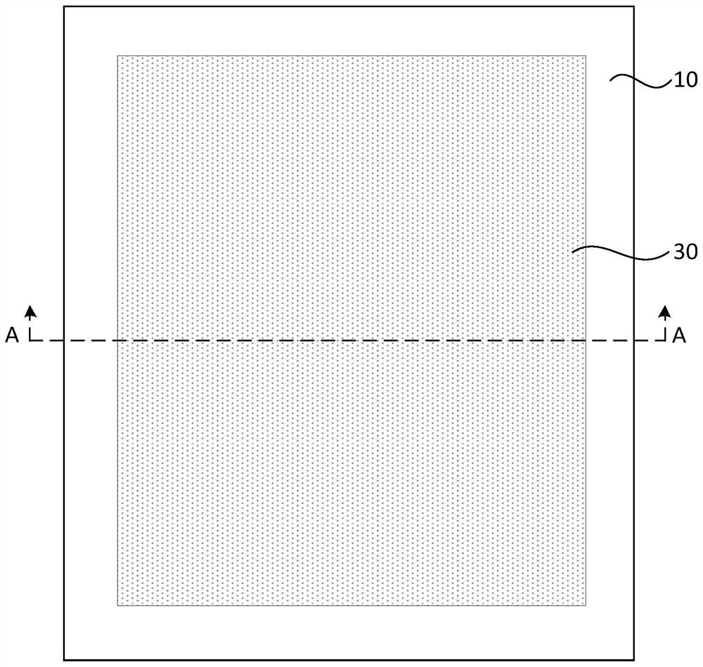
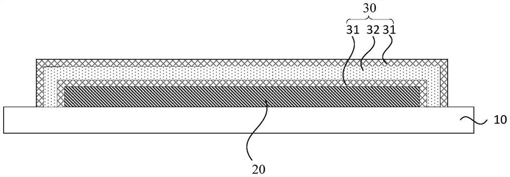
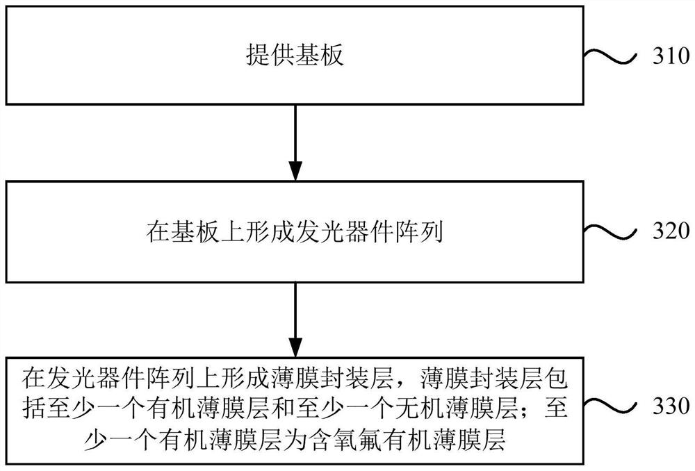
[0032] The present invention will be further described in detail below in conjunction with the accompanying drawings and embodiments. It should be understood that the specific embodiments described here are only used to explain the present invention, but not to limit the present invention. In addition, it should be noted that, for the convenience of description, only some structures related to the present invention are shown in the drawings but not all structures.

[0033] Example embodiments may be embodied in many forms and should not be construed as limited to the embodiments set forth herein; rather, these embodiments are provided so that this disclosure will be thorough and complete, and will fully convey the concepts of example embodiments to this disclosure. technical personnel in the field. The same reference numerals denote the same or similar structures in the drawings, and thus their repeated descriptions will be omitted. The words expressing position and directio...


PUM

PropertyMeasurementUnit
thicknessaaaaaaaaaa
thicknessaaaaaaaaaa
transmittivityaaaaaaaaaa

Abstract

The invention discloses an OLED panel, a preparation method of the OLED panel and a display device. The OLED panel includes a substrate; an array of light-emitting devices located on the substrate; a thin-film encapsulation layer that encapsulates the array of light-emitting devices, and the thin-film encapsulation layer includes at least one organic thin film layer and at least one inorganic thin film layer; at least one of the organic The film layer is an oxygen-fluorine organic film layer. The technical solution provided by the present invention uses an oxygen-fluorine-containing organic thin film layer to replace the organic thin film layer in the prior art, which can improve the light transmittance of the thin film encapsulation layer, especially the light transmittance of the blue light wavelength band, so that the thin film encapsulation layer reduces the Light transmission loss to light emitting devices.

Description

technical field [0001] The embodiments of the present invention relate to the technical field of OLED packaging, and in particular to an OLED panel, a method for manufacturing the OLED panel, and a display device. Background technique [0002] The optical materials and electrodes in OLED devices are very sensitive to water vapor and oxygen, and the penetration of water and oxygen will greatly reduce the life of OLED devices. In order to meet the requirements of commercialization for the service life and stability of OLED devices, OLED devices require packaging very high. Therefore, encapsulation is very important in OLED panel fabrication. [0003] Traditional encapsulation usually adopts cover plate encapsulation technology, coating the encapsulation glass with a UV-curable sealant, or applying a sealant and filling it with a desiccant. After the sealant is cured, it can provide a relatively airtight environment for the OLED device, thereby isolating water. Oxygen enters....

Claims


Application Information

Patent Timeline
Patent Type & Authority Patents(China)
IPC IPC(8): H01L51/52H01L51/56H01L27/32
CPCH10K59/00H10K50/84H10K71/00
Inventor 卢青
Owner JITRI INST OF ORGANIC OPTOELECTRONICS CO LTD
Why Eureka
Try Eureka