Check patentability & draft patents in minutes with Patsnap Eureka AI!

A manufacturing method of a heat dissipation package structure and a heat dissipation structure

A packaging structure and manufacturing method technology, which is applied in semiconductor/solid-state device manufacturing, semiconductor/solid-state device parts, semiconductor devices, etc., can solve the problems of large packaging volume, high cost, and poor heat dissipation, and achieve small packaging volume, Low cost, good cooling effect

Active Publication Date: 2022-07-12
NINGBO SEMICON INT CORP
View PDF7 Cites 0 Cited by
  • Summary
  • Abstract
  • Description
  • Claims
  • Application Information

AI Technical Summary

Problems solved by technology

[0005] The purpose of the present invention is to provide a method for manufacturing a heat dissipation packaging structure and a heat dissipation structure to solve the problems of large packaging volume, poor heat dissipation, and high cost

Method used


Image

  • A manufacturing method of a heat dissipation package structure and a heat dissipation structure
  • A manufacturing method of a heat dissipation package structure and a heat dissipation structure
  • A manufacturing method of a heat dissipation package structure and a heat dissipation structure

Examples


Embodiment Construction

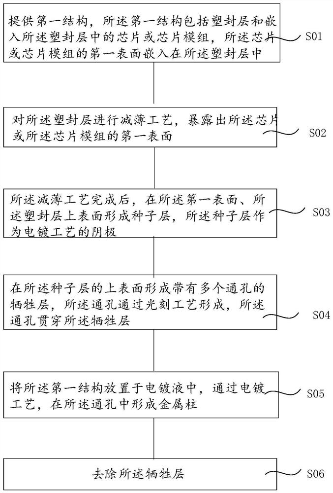
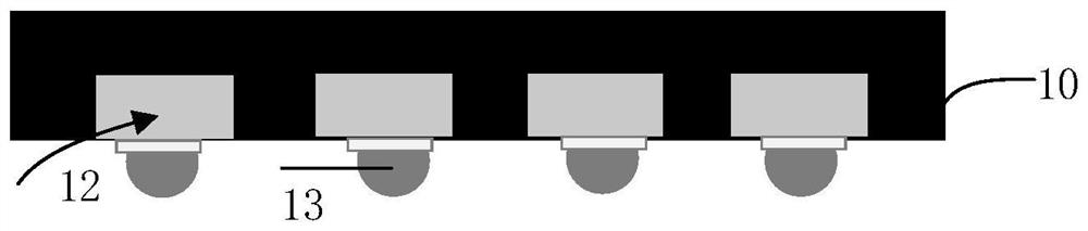
[0024] The present invention will be further described in detail below with reference to the accompanying drawings and specific embodiments. The advantages and features of the present invention will become clearer from the following description and accompanying drawings, however, it should be noted that the concept of the technical solution of the present invention can be implemented in various forms, and is not limited to the specific implementation described herein example. The accompanying drawings are all in a very simplified form and in an inaccurate scale, and are only used to facilitate and clearly assist the purpose of explaining the embodiments of the present invention.

[0025] It will be understood that when an element or layer is referred to as being "on," "adjacent to," "connected to," or "coupled to" other elements or layers, it can be directly on the other elements or layers Layers may be on, adjacent to, connected or coupled to other elements or layers, or int...


PUM

PropertyMeasurementUnit
thicknessaaaaaaaaaa
heightaaaaaaaaaa
thicknessaaaaaaaaaa

Abstract

The invention discloses a manufacturing method and a heat dissipation structure of a heat dissipation packaging structure. The manufacturing method comprises: providing a first structure, the first structure includes a plastic sealing layer and a chip embedded in the plastic sealing layer, and the first surface of the chip is embedded in the plastic sealing layer in the middle; perform a thinning process on the plastic sealing layer to expose the first surface of the chip; after the thinning process is completed, a seed layer is formed on the first surface and the upper surface of the plastic sealing layer, and the seed layer is used as the cathode of the electroplating process; on the seed layer A sacrificial layer with a plurality of through holes is formed on the surface, the through holes are formed by a photolithography process, and the through holes penetrate through the sacrificial layer; the first structure is placed in an electroplating solution, and a heat dissipation column is formed in the through holes through an electroplating process; Floor. The beneficial effects of the present invention are: forming a through hole on the sacrificial layer through a photolithography process, and forming a plurality of heat dissipation columns in the through hole through an electroplating process, and reducing the cost of the heat dissipation structure while ensuring the heat dissipation effect.

Description

technical field [0001] The invention relates to the field of semiconductor device packaging, in particular to a manufacturing method of a heat dissipation packaging structure and a heat dissipation structure. Background technique [0002] With the improvement of the function and processing speed of electronic products, the semiconductor chip, which is the core component of the electronic product, needs to have higher density electronic components, and the semiconductor chip will generate a larger amount of heat energy when it operates, and the heat dissipation of the chip has become a important topic. Chips in the package structure usually rely on additional heat dissipation devices to achieve better heat dissipation, but the production cost and package thickness are increased. [0003] The current solution is to form a plurality of through holes in the plastic sealing layer on the back of the chip through an etching process, and deposit a metal film layer in the through ho...

Claims


Application Information

Patent Timeline
Patent Type & Authority Patents(China)
IPC IPC(8): H01L21/48H01L23/367H01L23/373
CPCH01L21/4871H01L23/367H01L23/3736
Inventor 狄云翔
Owner NINGBO SEMICON INT CORP
Features
  • R&D
  • Intellectual Property
  • Life Sciences
  • Materials
  • Tech Scout
  • Unparalleled Data Quality
  • Higher Quality Content
  • 60% Fewer Hallucinations
Learn More