

Voltage conversion circuit and display device
Patent Information
- Authority / Receiving Office
- CN · China
- Patent Type
- Patents(China)
- Current Assignee / Owner
- TCL CHINA STAR OPTOELECTRONICS TECH CO LTD
- Publication Date
- 2022-04-01
Smart Images
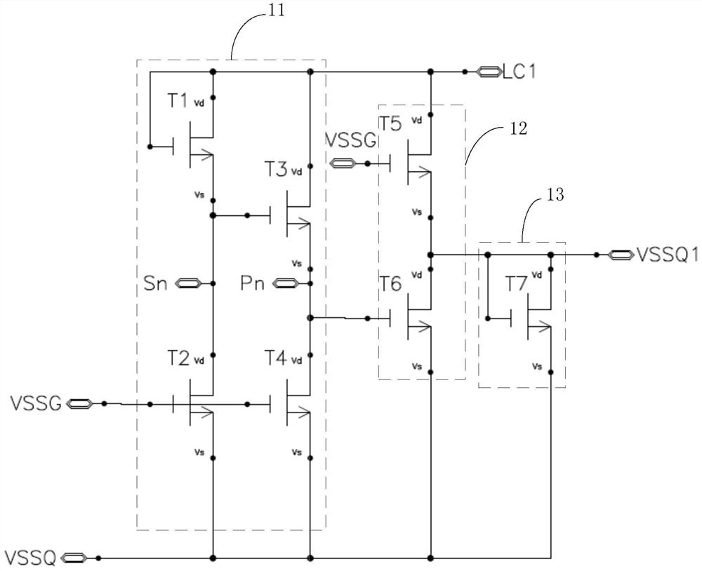
Figure 1 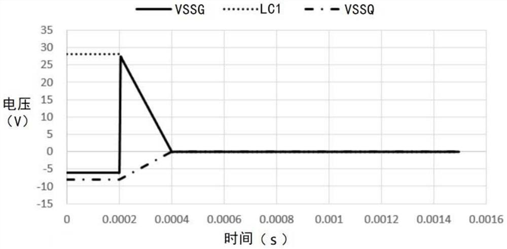
Figure 2 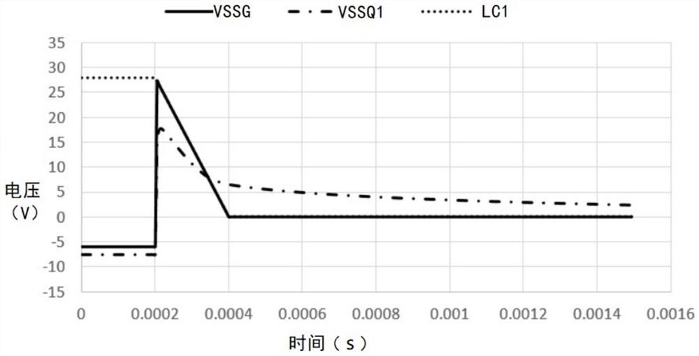
Figure 3
Abstract
Description
technical field
[0001] The invention relates to the technical field of display panels, in particular to a voltage conversion circuit and a display device. Background technique
[0002] At present, due to the difference in the design structure of the LCD panel, a new negative voltage VSSQ signal is added to the GOA (Gate Driver On Array, gate drive circuit) signal to improve the leakage of the pixel drive transistor and improve the reliability of the GOA circuit.
[0003] However, the original IC does not support discharge output of multiple VSS signals (multiple VSS signals include VSSG signal and VSSQ signal). The GOA circuit cannot drive the pixel drive transistor to turn on, and the residual charge on the pixel electrode cannot be released, which leads to afterimage after shutdown. Contents of the invention
[0004] Embodiments of the present invention provide a voltage conversion circuit and a display panel, so as to solve the problem of afterimage after power-off cau...