Array substrate and driving method thereof, and display device

A technology for array substrates and display devices, applied to static indicators, instruments, etc., can solve problems such as after-image after shutdown and panel image residue, and achieve the effect of improving display quality and eliminating after-image after shutdown

Active Publication Date: 2015-08-12
HEFEI BOE OPTOELECTRONICS TECH +1
View PDF6 Cites 0 Cited by
  • Summary
  • Abstract
  • Description
  • Claims
  • Application Information

AI Technical Summary

Problems solved by technology

[0004] However, since AMOLED is an active driving method, there will be charge left on the pixel capacitor at the moment of shutdown, and these charges will keep the pixel at the voltage before shutdown at the moment of shutdown, so that the panel will have residual images, forming the so-called shutdown residue. film

Method used


Image

  • Array substrate and driving method thereof, and display device
  • Array substrate and driving method thereof, and display device
  • Array substrate and driving method thereof, and display device

Examples


Embodiment Construction

[0019] The following will clearly and completely describe the technical solutions in the embodiments of the present invention with reference to the accompanying drawings in the embodiments of the present invention. Obviously, the described embodiments are only some, not all, embodiments of the present invention. Based on the embodiments of the present invention, all other embodiments obtained by persons of ordinary skill in the art without making creative efforts belong to the protection scope of the present invention.

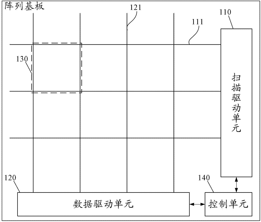
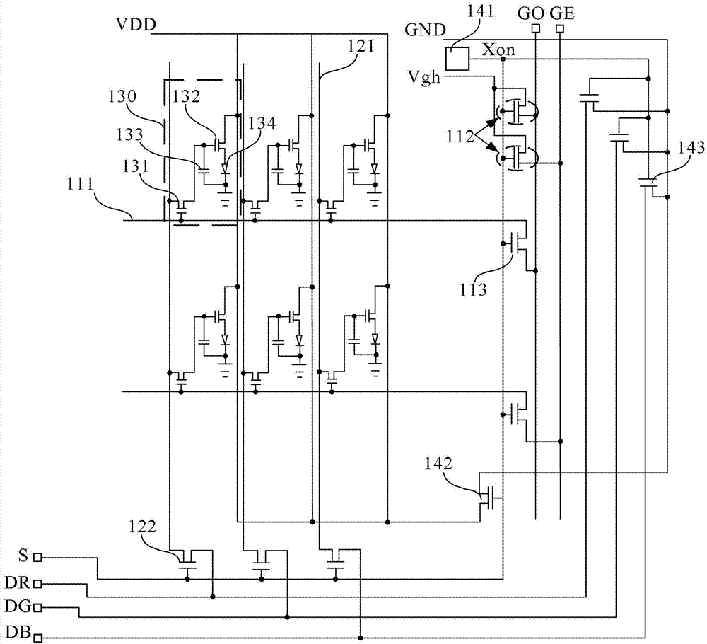
[0020] An embodiment of the present invention provides an array substrate, such as figure 1 As shown, it includes: a scanning driving unit 110 for providing row scanning signals to a plurality of gate lines 111, a data driving unit 120 for providing data signals to a plurality of data lines 121, a plurality of gate lines 111 and a plurality of data lines Lines 121 intersect horizontally and vertically to form an array of pixel units 130 arranged in a matrix, w...


PUM


Abstract

An array substrate includes: a scanning driving unit for providing a row scanning signal to a plurality of gate lines, and a data driving unit for providing a data signal to a plurality of data lines, the plurality of gate lines and the plurality of data lines being horizontally and vertically crossed to form an array of pixel units arranged in an matrix form, and further including: a control unit electrically connected with the scanning driving unit and the data driving unit respectively, for controlling the scanning driving unit turn on each of the pixel units when the display device is powered off, such that charges stored in the pixel units are rapidly discharged through the data lines, so as to eliminate the shutdown image sticking of the AMOLED display. There have disclosed also a method for driving array substrate and a display device.

Description

technical field [0001] The present invention relates to the field of display technology, in particular to an array substrate, a driving method thereof, and a display device. Background technique [0002] The principle of OLED (Organic Light Emitting Diode) display is to apply a certain electric field to the anode and cathode on both sides of the electroluminescent layer. Driven by the electric field, electrons and holes pass through the cathode and anode respectively. The transport layer and the hole transport layer migrate to the emissive layer, where they meet to form excitons and excite light-emitting molecules, which undergo radiative relaxation to emit visible light. Compared with traditional LCD (Liquid Crystal Display, liquid crystal display), OLED display is more and more used in high performance display field. [0003] According to the driving method, OLED can be divided into two types: PMOLED (Passive Matrix Driving OLED, passive matrix driving organic light emit...

Claims


Application Information

Patent Timeline
Patent Type & Authority Patents(China)
IPC IPC(8): G09G3/32
CPCG09G2300/0426G09G3/3233G09G2320/0257G09G3/3266G09G2330/027G09G2310/0245
Inventor 徐向阳
Owner HEFEI BOE OPTOELECTRONICS TECH
Why Eureka
Try Eureka