Nanometer titanium dioxide film and preparation method thereof, and preparation method of photoelectric device

A technology of nano-titanium dioxide and thin film, which is applied in the fields of electrical solid-state devices, semiconductor/solid-state device manufacturing, nanotechnology, etc., can solve the problems of poor uniformity and poor compactness of the nano-titanium dioxide electron transport layer film, and achieve improved photoelectric efficiency, surface compactness, The effect of increasing the migration rate

Pending Publication Date: 2022-01-11
TCL CORPORATION
View PDF1 Cites 1 Cited by
  • Summary
  • Abstract
  • Description
  • Claims
  • Application Information

AI Technical Summary

Problems solved by technology

[0004] The purpose of this application is to provide a nano-titanium dioxide thin film and its preparation method, as well as a method for preparing a photoelectric device, aiming to solve the problem of poor uniformity and poor compactness of the nano-titanium dioxide electron transport layer film prepared by the existing method to a certain extent

Method used


Image

  • Nanometer titanium dioxide film and preparation method thereof, and preparation method of photoelectric device
  • Nanometer titanium dioxide film and preparation method thereof, and preparation method of photoelectric device
  • Nanometer titanium dioxide film and preparation method thereof, and preparation method of photoelectric device

Examples


preparation example Construction

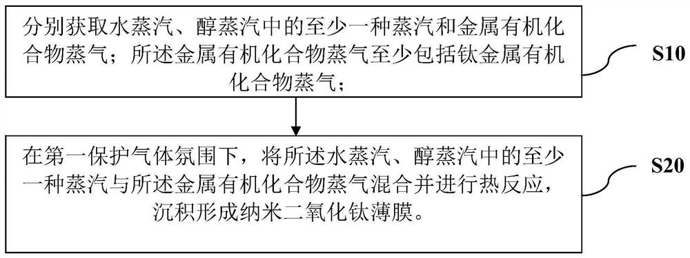
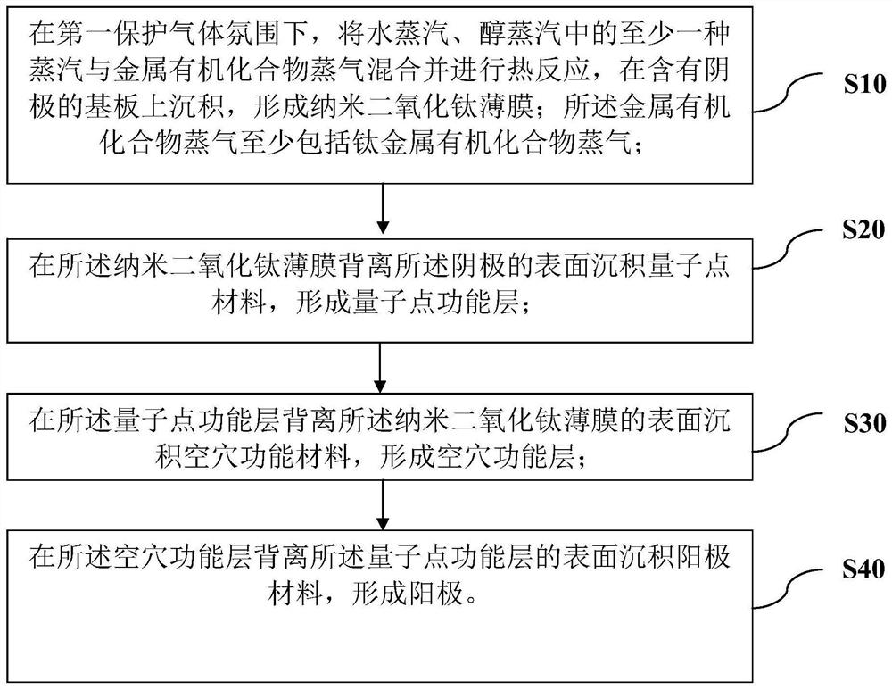
[0029] as attached figure 1 As shown, the first aspect of the embodiment of the present application provides a method for preparing a nano-titanium dioxide film, comprising the following steps:

[0030] S10. Obtaining at least one of water vapor, alcohol vapor, and metal-organic compound vapor respectively; the metal-organic compound vapor includes at least titanium metal-organic compound vapor;

[0031] S20. Under the atmosphere of the first protective gas, at least one vapor of water vapor and alcohol vapor is mixed with metal-organic compound vapor and thermally reacted to deposit and form a nano-titanium dioxide film.

[0032]The first aspect of the present application provides a method for preparing a nano-titanium dioxide film, using titanium metal organic compound vapor and water vapor and / or alcohol vapor as reaction raw materials, so that each raw material component reacts in a gas phase state, and each raw material component can be more uniform The distribution and ...

Embodiment 1

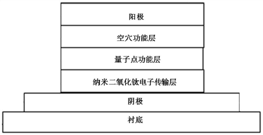
[0085] (1) A nano-titanium dioxide electron transport layer, comprising the steps of:

[0086] The cleaned ITO conductive glass substrate is transferred to the furnace body of the vapor deposition furnace, and high-purity argon gas is introduced to remove the air in the furnace body. Next, the temperature of the furnace body was raised and stabilized at 550°C. Then, add butyl titanate and deionized water into the steam generator, and adjust the temperature of butyl titanate and deionized water to 115°C and 100°C respectively, and wait for the temperature of butyl titanate and deionized water to stabilize , switch the protective gas circuit, make the high-purity argon flow into the steam generating device respectively equipped with butyl titanate and deionized water at a flow rate of 100ml / min, and generate corresponding butyl titanate steam and water vapor by bubbling. Steam is loaded into the vapor deposition furnace body. After continuing the reaction for 30 minutes, switc...

Embodiment 2

[0092] (1) A nano-titanium dioxide electron transport layer, comprising the steps of:

[0093] The cleaned ITO conductive glass substrate is transferred to the furnace body of the vapor deposition furnace, and high-purity argon gas is introduced to remove the air in the furnace body. Next, the temperature of the furnace body was raised and stabilized at 550°C. Then, add isopropyl titanate and deionized water into the steam generator, and adjust the temperature of isopropyl titanate and deionized water to 105°C and 100°C respectively. After the temperature stabilizes, switch the protective gas circuit so that the high-purity argon enters the steam generating device equipped with isopropyl titanate and deionized water at a flow rate of 100ml / min, and generates corresponding isopropyl titanate steam and steam, and load the steam into the vapor deposition furnace body. After continuing to react for 30 minutes, switch the gas path, turn off the steam generator, and stop the loadi...


PUM

PropertyMeasurementUnit
thicknessaaaaaaaaaa
particle diameteraaaaaaaaaa
thicknessaaaaaaaaaa

Abstract

The invention belongs to the technical field of display devices, and particularly relates to a preparation method of a nano titanium dioxide film. The method comprises the following steps: respectively obtaining at least one of water vapor and alcohol vapor and metal organic compound vapor, wherein the metal organic compound steam at least comprises titanium metal organic compound steam; and in a first protective gas atmosphere, mixing at least one of the water vapor and the alcohol vapor with the metal organic compound vapor, carrying out thermal reaction, and depositing to form the nano titanium dioxide film. According to the preparation method, gas-phase free nano titanium dioxide particles are generated through reaction of gas-phase raw materials and deposited to form the thin film, the thin film is firmly combined with the substrate, and the formed thin film is compact in surface and good in film layer uniformity. Besides, by controlling the deposition time of the free nano titanium dioxide particles, the thickness of the formed nano titanium dioxide film can be flexibly regulated and controlled, the operation is simple and flexible, and the invention is suitable for industrial large-scale production and application.

Description

technical field [0001] The application belongs to the technical field of display devices, and in particular relates to a nano-titanium dioxide thin film, a preparation method thereof, and a photoelectric device preparation method. Background technique [0002] Quantum dot materials are considered to be new optoelectronic materials with great potential due to their optical characteristics such as wide excitation spectrum, narrow emission spectrum, adjustable emission wavelength, and high luminous efficiency. In a high-efficiency quantum dot solar cell, the basic structure of the cell includes glass, ITO, an electron transport layer, a light absorption sensitization layer, a hole transport layer, and a metal electrode. As the most commonly used material for electron transport layer components, nano-titanium dioxide film has the characteristics of non-toxic and environmentally friendly, high transparency, and good light stability. Nevertheless, there are still many limiting fa...

Claims


Application Information

Patent Timeline
Patent Type & Authority Applications(China)
IPC IPC(8): H01L51/50H01L51/54H01L51/56B82Y30/00B82Y40/00
CPCB82Y30/00B82Y40/00H10K50/115H10K50/16H10K2102/00H10K71/00
Inventor 丘洁龙
Owner TCL CORPORATION
Why Eureka
Try Eureka