Display substrate, manufacturing method, display device, detection method and detection device

A display substrate and display area technology, which is applied in the direction of static indicators, semiconductor/solid-state device manufacturing, instruments, etc., can solve the problems that the encapsulation layer of the OLED substrate is prone to failure, etc., so as to improve the overall reliability, prevent display abnormalities, and widely The effect of applying the foreground

Pending Publication Date: 2022-07-05
BOE TECH GRP CO LTD
View PDF0 Cites 0 Cited by
  • Summary
  • Abstract
  • Description
  • Claims
  • Application Information

AI Technical Summary

Problems solved by technology

The commonly used packaging method for this type of display substrate is the method of thin film pac

Method used


Image

  • Display substrate, manufacturing method, display device, detection method and detection device
  • Display substrate, manufacturing method, display device, detection method and detection device
  • Display substrate, manufacturing method, display device, detection method and detection device

Examples


Embodiment Construction

[0072] In order to illustrate the present invention more clearly, the present invention will be further described below with reference to the embodiments and accompanying drawings. Similar parts in the figures are denoted by the same reference numerals. Those skilled in the art should understand that the content specifically described below is illustrative rather than restrictive, and should not limit the protection scope of the present invention.

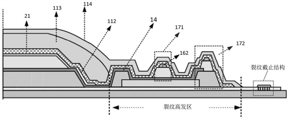
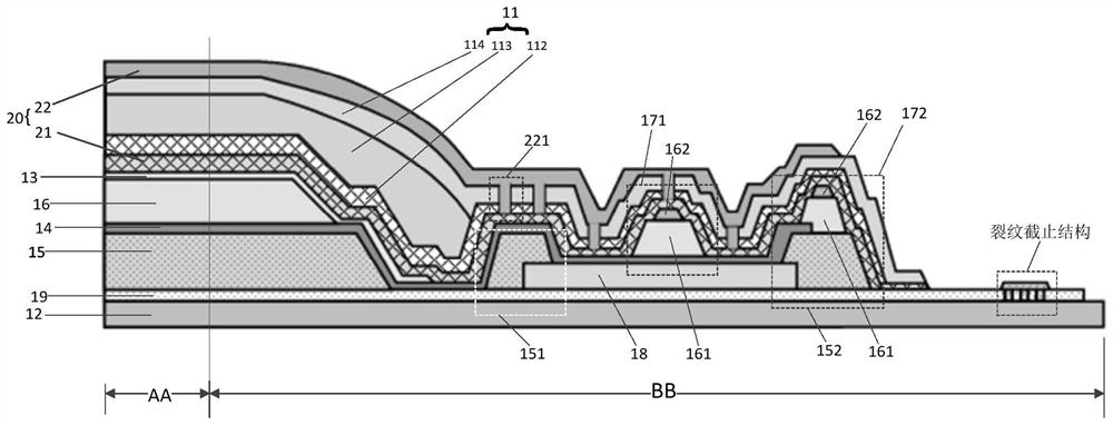
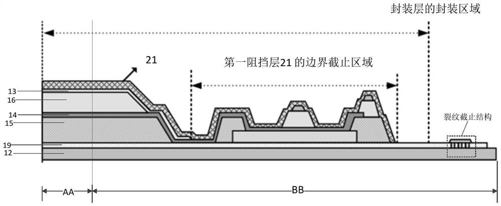
[0073] In related technologies, such as figure 1 As shown, the encapsulation layer of the display substrate mostly adopts the stacked structure of inorganic layer and organic layer, which is realized by plasma-enhanced chemical vapor deposition (PECVD), sputtering process (SUPTTER), atomic layer deposition (ALD) and other methods. The preparation of the inorganic layer of the encapsulation layer, the inorganic layer is used to block the invasion of water and oxygen from the outside. Due to the large stress in the inorganic layer,...


PUM


Abstract

The invention discloses a display substrate, a manufacturing method, a display device, a detection method and a detection device. According to one embodiment, the display substrate comprises a display area, a non-display area surrounding the display area and a packaging layer packaging the display area and the non-display area. The display substrate further comprises a crack blocking structure, and the first projection cover of the packaging layer on the substrate of the display substrate is at least partially overlapped with the projection of the crack blocking structure on the substrate. According to the technical scheme, the crack blocking structure is arranged on the display substrate, and the first projection of the packaging layer on the substrate is at least partially overlapped with the projection of the crack blocking structure on the substrate, so that the crack blocking structure overlapped with the first projection of the packaging layer is used for protecting the packaging layer; the problem of abnormal display caused by cracks of the packaging layer is prevented, the overall reliability of the display panel is improved, and the display panel has a wide application prospect.

Description

technical field [0001] The present invention relates to the field of display technology. More specifically, it relates to a display substrate, a manufacturing method, a display device, a detection method, and a detection device. Background technique [0002] Currently, bendable displays can be realized by liquid crystal display (LCD) and organic light emitting diode (OLED) display panels. Among them, benefiting from the characteristics of self-luminescence, it is easier to fabricate an OLED display on a flexible substrate to achieve a bendable display with a smaller bending radius. Therefore, the fabrication of OLED display panels including flexible substrates has attracted extensive attention. The commonly used packaging method for this type of display substrate is the method of using thin film packaging, but the accompanying problem is that the packaging layer of the OLED substrate is prone to failure. SUMMARY OF THE INVENTION [0003] The purpose of the present inven...

Claims


Application Information

Patent Timeline
IPC IPC(8): H01L51/52H01L51/56G09G3/00H01L27/32
CPCG09G3/006H10K59/12H10K50/84H10K50/844H10K71/00
Inventor 王涛
Owner BOE TECH GRP CO LTD
Why Eureka
Try Eureka