Power amplifier circuit and power amplifier module
a power amplifier circuit and power amplifier technology, applied in the direction of amplifier combinations, high frequency amplifiers, gated amplifiers, etc., can solve the problems of power loss and increase the power consumption of the power amplifier circuit, and achieve the effect of reducing radio frequency signal loss
- Summary
- Abstract
- Description
- Claims
- Application Information
AI Technical Summary
Benefits of technology
Problems solved by technology
Method used
Image

Examples
first embodiment
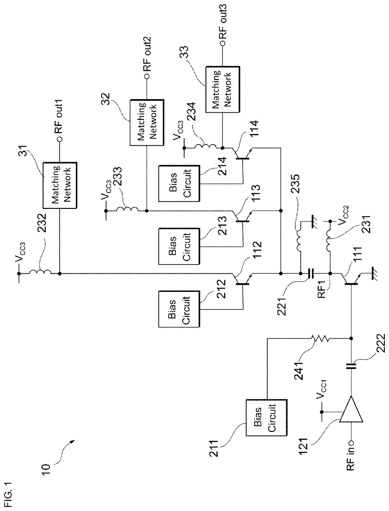
[0027]A first embodiment will be described. As illustrated in FIG. 1, a power amplifier circuit 10 includes transistors 111, 112, 113, and 114, an amplifier 121, bias circuits 211, 212, 213, and 214, capacitors 221 and 222, inductors 231, 232, 233, 234, and 235, a resistance element 241, and matching networks 31, 32, and 33.
[0028]Each of the transistors 111, 112, 113, and 114 is, for example, a transistor, such as a heterojunction bipolar transistor (HBT). In the present disclosure, each transistor is not limited to a heterojunction bipolar transistor, and another transistor, such as a field-effect transistor (FET), may be used.
[0029]A power-supply voltage Vcc2 is supplied to a collector of the transistor 111 through the inductor 231. A base of the transistor 111 is connected to the bias circuit 211 through the resistance element 241 and is connected to the amplifier 121 through the capacitor 222. An emitter of the transistor 111 is connected to a ground.
[0030]A power-supply voltage...
second embodiment
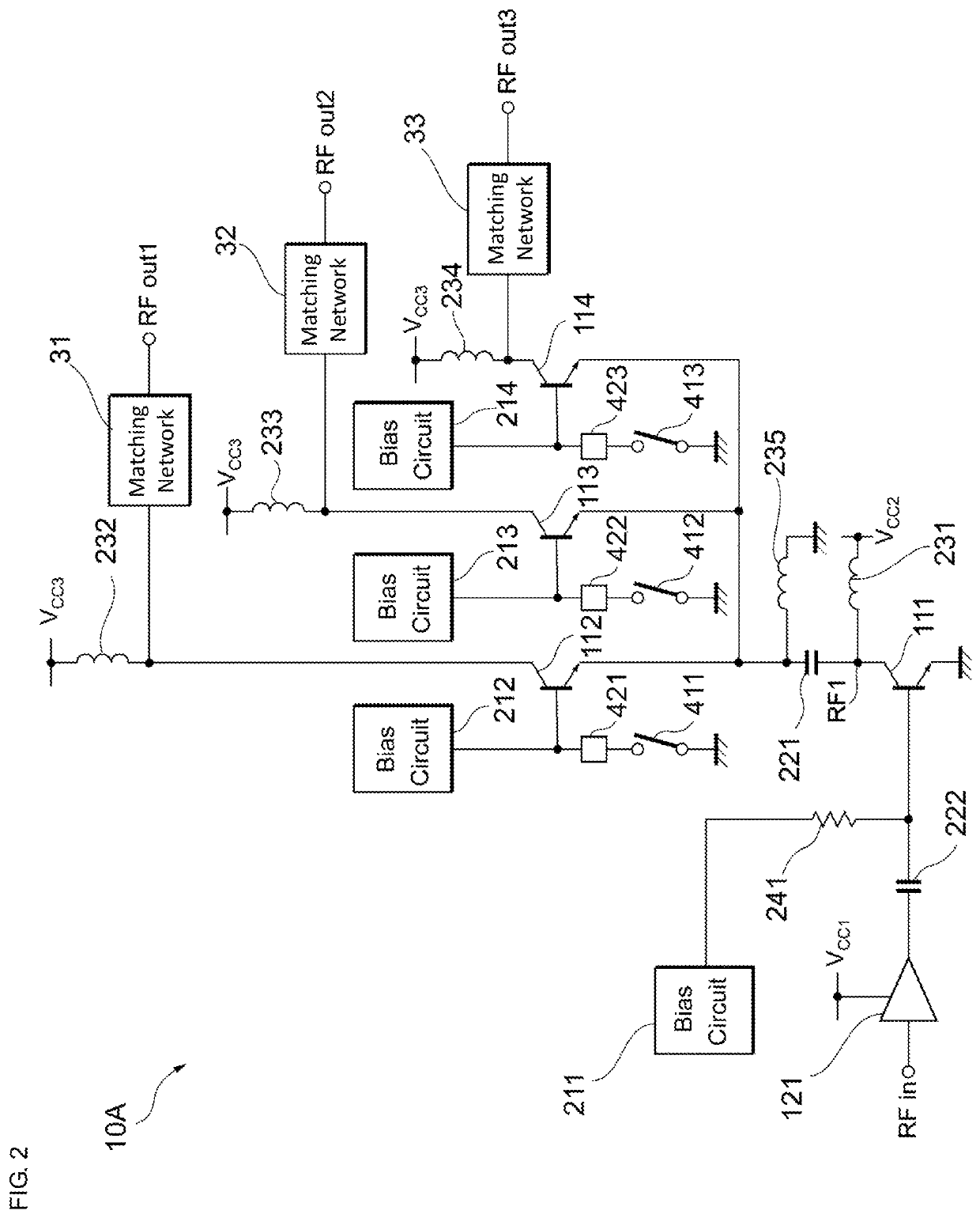
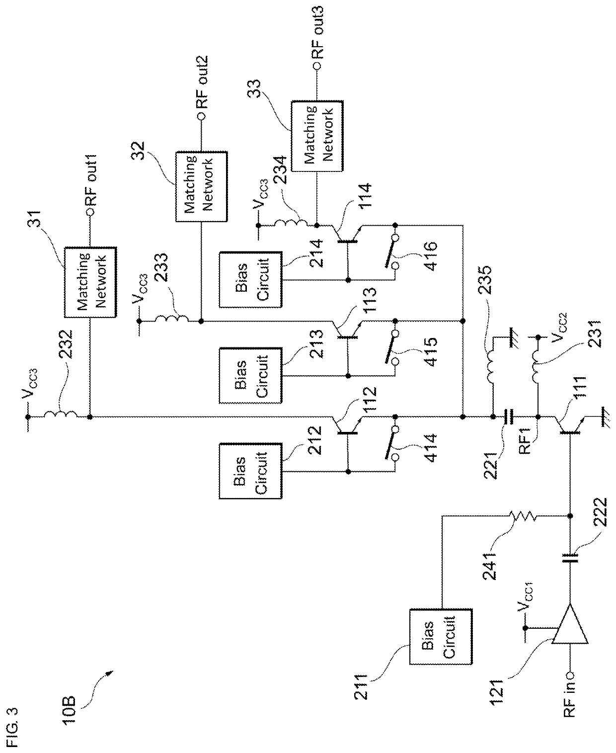
[0047]As illustrated in FIG. 2, a power amplifier circuit 10A further includes, in the power amplifier circuit 10, switches 411, 412, and 413, and impedance elements 421, 422, and 423.
[0048]One ends of the respective switches 411, 412, and 413 are connected to the ground. The impedance elements 421, 422, and 423 are connected in series with the respective other ends of the switches 411, 412, and 413. One ends of the impedance elements 421, 422, and 423 are connected to the respective bases of the transistors 112, 113, and 114.
[0049]Each of the impedance elements 421, 422, and 423 is an element configured to have a certain impedance. For example, each of the impedance elements 421, 422, and 423 is constituted by a resistor, an inductor, a composite of a resistor and an inductor, or the like.
[0050]With respect to the switches 411, 412, and 413, when a bias current or voltage is supplied to the base of the transistor 112, the switch 411 can be turned off, and the switches 412 and 413 ...
fourth embodiment
[0114]In the fourth embodiment, although the power amplifier circuit 10 includes three outputs, the number of outputs is not limited to three. As the number of output terminals increases or decreases, the number of duplexer blocks can be increased or reduced. For example, when the number of duplexer blocks 71 is adjusted as the duplexer block 72 is added, the number of frequency bands supported by the power amplifier module 20 can be increased or reduced.
[0115]Furthermore, with respect to switching of an amplified signal by the duplexer block 71 according to the fourth embodiment, any multi-output power amplifier circuit including multiple outputs that are selectively enabled can be used in this embodiment.
[0116]Among multiple transmission filters to which the same output is supplied, even if an amplified signal passes through mainly a certain transmission filter, there is a signal that passes through another filter. With reference to FIGS. 9 and 10, the influence of insertion loss ...
PUM
 Abstract
Description
Claims
Application Information
 - R&D
- Intellectual Property
- Life Sciences
- Materials
- Tech Scout
- Unparalleled Data Quality
- Higher Quality Content
- 60% Fewer Hallucinations
Browse by: Latest US Patents, China's latest patents, Technical Efficacy Thesaurus, Application Domain, Technology Topic, Popular Technical Reports.
© 2025 PatSnap. All rights reserved.Legal|Privacy policy|Modern Slavery Act Transparency Statement|Sitemap|About US| Contact US: help@patsnap.com