Display device and method for manufacturing the same

a technology of display device and manufacturing method, which is applied in the direction of semiconductor devices, organic semiconductor devices, electrical devices, etc., can solve the problems of reducing the efficiency of manufacturing process, and achieve the effect of improving process efficiency and improving luminous efficiency

US11411066B2Active Publication Date: 2022-08-09SAMSUNG DISPLAY CO LTD
9 Cites 0 Cited by

Patent Information

Authority / Receiving Office
US · United States
Patent Type
Patents(United States)
Current Assignee / Owner
Publication Date
2022-08-09

Smart Images

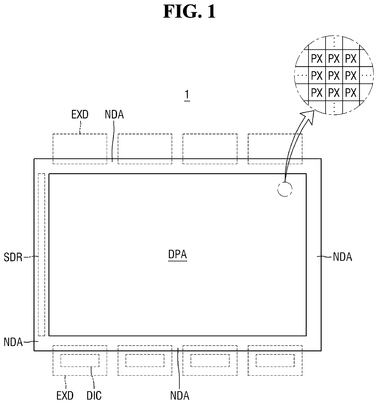
  • Figure 1
    Figure 1
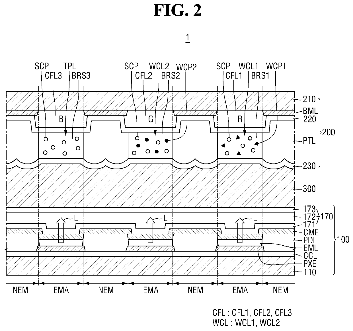
  • Figure 2
    Figure 2
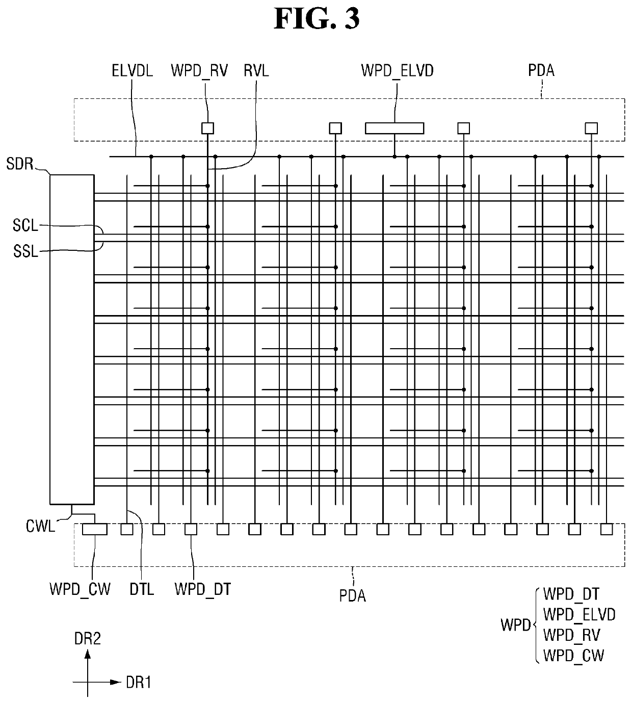
  • Figure 3
    Figure 3
Patent Text Reader

Abstract

A display device and a method of the display device are provided. The display device includes a lower metal layer on a substrate, a buffer layer on the lower metal layer, a first semiconductor layer on the buffer layer, a gate insulating layer on the first semiconductor layer, a first gate electrode on the gate insulating layer, an interlayer insulating layer on the first gate electrode, a via layer on the interlayer insulating layer, a pixel electrode on the via layer and electrically connected to the first semiconductor layer, a light emitting layer on the pixel electrode, a common electrode on the light emitting layer, a first contact hole penetrating the buffer layer and the interlayer insulating layer and a second contact hole penetrating the interlayer insulating layer, and a first via hole and a second via hole each penetrating the via layer.
Need to check novelty before this filing date? Find Prior Art

Description

CROSS-REFERENCE TO RELATED APPLICATION(S)

[0001] This application claims priority to and benefits of Korean Patent Application No. 10-2019-0179846 under 35 U.S.C. § 119, filed on Dec. 31, 2019, in the Korean Intellectual Property Office, the entire contents of which are incorporated herein by referenceBACKGROUND1. Technical Field

[0002] The disclosure relates to a display device and a method for manufacturing the display device, and more specifically, to a display device and a manufacturing method thereof with a process of improved efficiency.2. Description of the Related Art

[0003] The importance of display devices has steadily increased together with the development of multimedia technology. Various types of display devices such as a liquid crystal display (LCD), an organic light emitting display (OLED) and the like have been developed and used.

[0004] Among them, the organic light emitting display is a self-light emitting device that emits light by itself and has advantages such as fast ...

Examples

Embodiment Construction

[0045]The invention will now be described more fully hereinafter with reference to the accompanying drawings, in which embodiments of the invention are shown. This invention may, however, be embodied in different forms and should not be construed as limited to the embodiments set forth herein. Rather, these embodiments are provided so that this disclosure will be thorough and complete, and will fully convey the scope of the invention to those skilled in the art.

[0046]Some of the parts which are not associated with the description may not be provided to describe embodiments of the invention and like reference numerals refer to like elements throughout the specification.

[0047]In the drawings, sizes, thicknesses, and roughness of elements may be enlarged for clarity and ease of description thereof. However, the invention is not limited to the illustrated sizes and thicknesses. In the drawings, the thicknesses of layers, films, panels, regions, and other elements may be exaggerated for ...