

Silicon wafer
- Summary
- Abstract
- Description
- Claims
- Application Information
AI Technical Summary
Benefits of technology
Problems solved by technology
Method used
Image

Examples
example 1
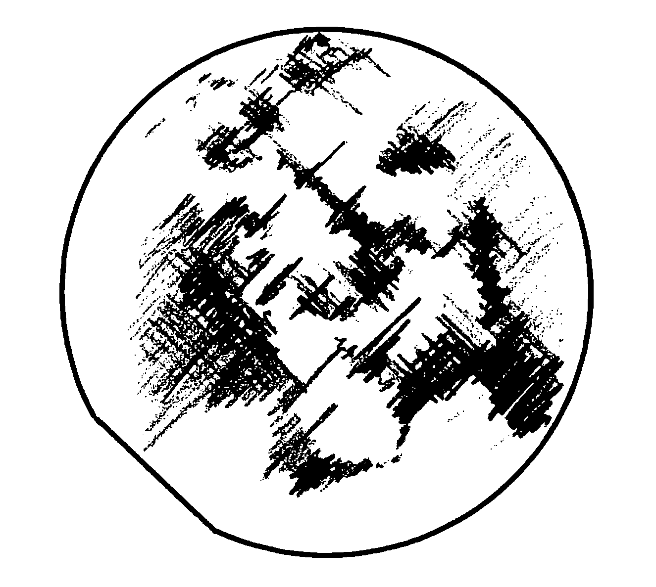
[0059] In the processes for a growth of a silicon single crystalline ingot by the Czochralski method, we employed a process (1) in which a silicon of liquid phase was doped with a predetermined amount of boron as well as a predetermined amount of germanium, and a silicon single crystal having a diameter of 150 mm was grown. We employed also another process (2) in which a silicon of liquid phase was doped with boron, germanium and carbon each by a predetermined amount, and a silicon single crystal having a diameter of 150 mm was grown. For the measurement of the concentration of boron, germanium and carbon, the Secondary Ion Mass Spectrometer (SIMS) was used. Each one of the silicon single crystal ingots fabricated by the processes (1) and (2) was sliced into a silicon wafer, which in turn was processed according to an established procedure by applying a sequence of steps consisting of chamfering, lapping, acid etching and mirror polishing to be formed into the silicon wafer. Subsequ...
example 2
[0065] Subsequently, we had made a research to see the effect on the crystal yield of adding boron of high concentration and germanium of high concentration altogether at the same time during the growth of the silicon single crystalline ingot by the CZ method. Specifically, the concentration ratios of boron and germanium were changed, and a plurality of silicon single crystal ingots of 150 mm diameter having different concentration ratios (n pieces=each 4 pieces) were grown, on which the occurrence of the first dislocation generation was observed. The results are shown in Table-2. In the table, .largecircle. indicates the case where the silicon single crystal has grown without any dislocation along the full length thereof and X indicates the case where the dislocation has occurred in the silicon single crystal in the course of the growth of the single crystal.
2 TABLE 2 Boron Occurrence of dislocation Boron Germanium concentration / in single crystal concentration concentration German...
PUM
 Abstract
Description
Claims
Application Information