

Integrated circuit design for signal integrity, avoiding well proximity effects
a technology of integrated circuits and signal integrity, applied in the direction of program control, total factory control, instruments, etc., can solve the problems of time-consuming and resource-intensive approaches, not desirable placement,
- Summary
- Abstract
- Description
- Claims
- Application Information
AI Technical Summary
Benefits of technology
Problems solved by technology
Method used
Image

Examples
Embodiment Construction
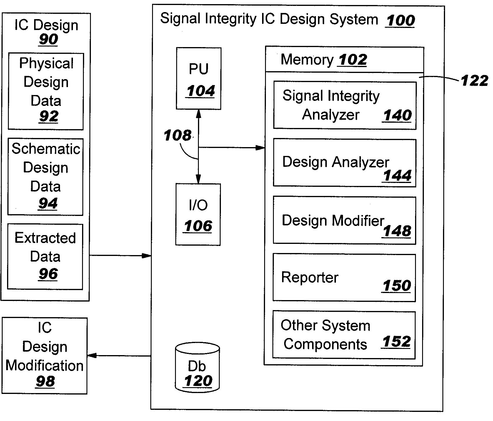
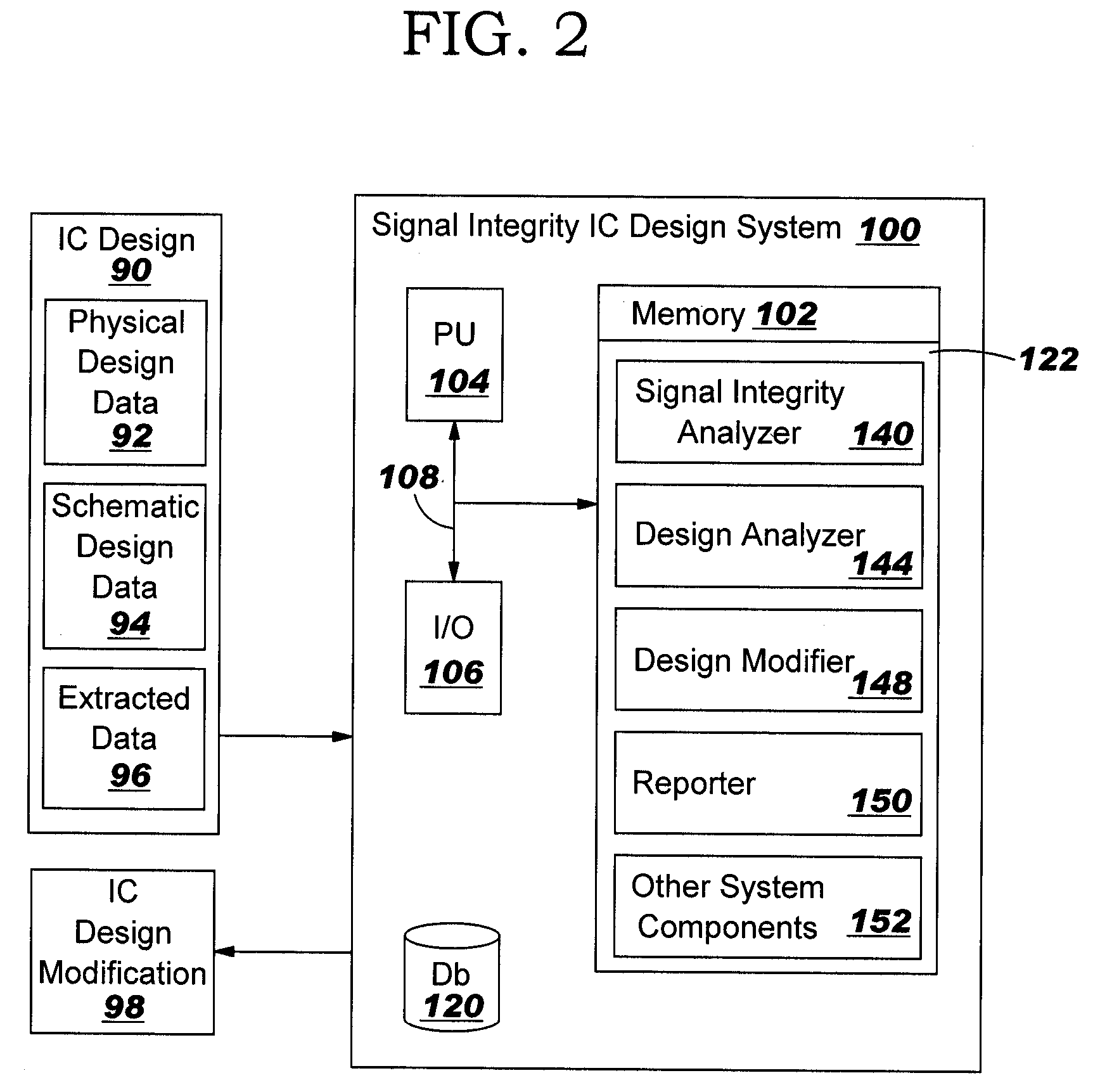
[0013] With reference to the accompanying drawings, FIG. 2 is a block diagram of a signal integrity IC design system 100 in accordance with the invention. Design system 100 includes a memory 102, a processing unit (PU) 104, input / output devices (I / O) 106 and a bus 108. A database 120 may also be provided for storage of data relative to processing tasks. It should be recognized that even though system 100 will be described in terms of a separate system, the teachings of the invention are equally applicable where system 100 is part of a larger IC design system (not shown).
[0014] Memory 102 includes a program product 122 that, when executed by PU 104, comprises various functional capabilities described in further detail below. Memory 102 (and database 120) may comprise any known type of data storage system and / or transmission media, including magnetic media, optical media, random access memory (RAM), read only memory (ROM), a data object, etc. Moreover, memory 102 (and database 120) m...
PUM
 Abstract
Description
Claims
Application Information