
Method for forming photoresist layer on subsrtate and bumping process using the same
a photoresist layer and substrate technology, applied in the direction of electrical equipment, semiconductor devices, semiconductor/solid-state device details, etc., can solve the problems of shortening the pitch of neighboring pads, the general surface of the passivation layer is not ideal, etc., to achieve the effect of improving the joining
- Summary
- Abstract
- Description
- Claims
- Application Information
AI Technical Summary
Benefits of technology
Problems solved by technology
Method used
Image

Examples
Embodiment Construction
[0025] Reference will now be made in detail to the present preferred embodiments of the invention, examples of which are illustrated in the accompanying drawings. Wherever possible, the same reference numbers are used in the drawings and the description to refer to the same or like parts.
[0026] In the embodiments of the present invention, a method for forming a photoresist layer on a substrate and a bumping process using the same are illustrated, which can prevent solder bridging between two neighboring pads.
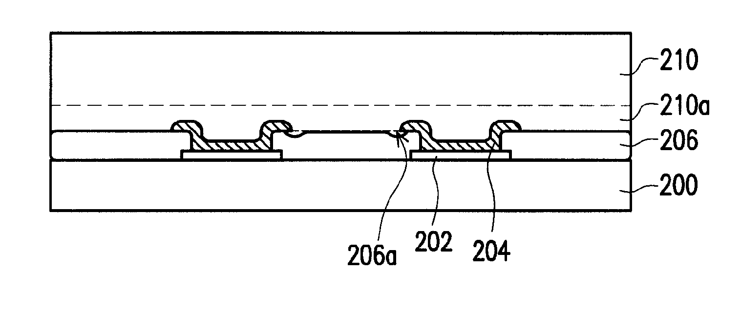
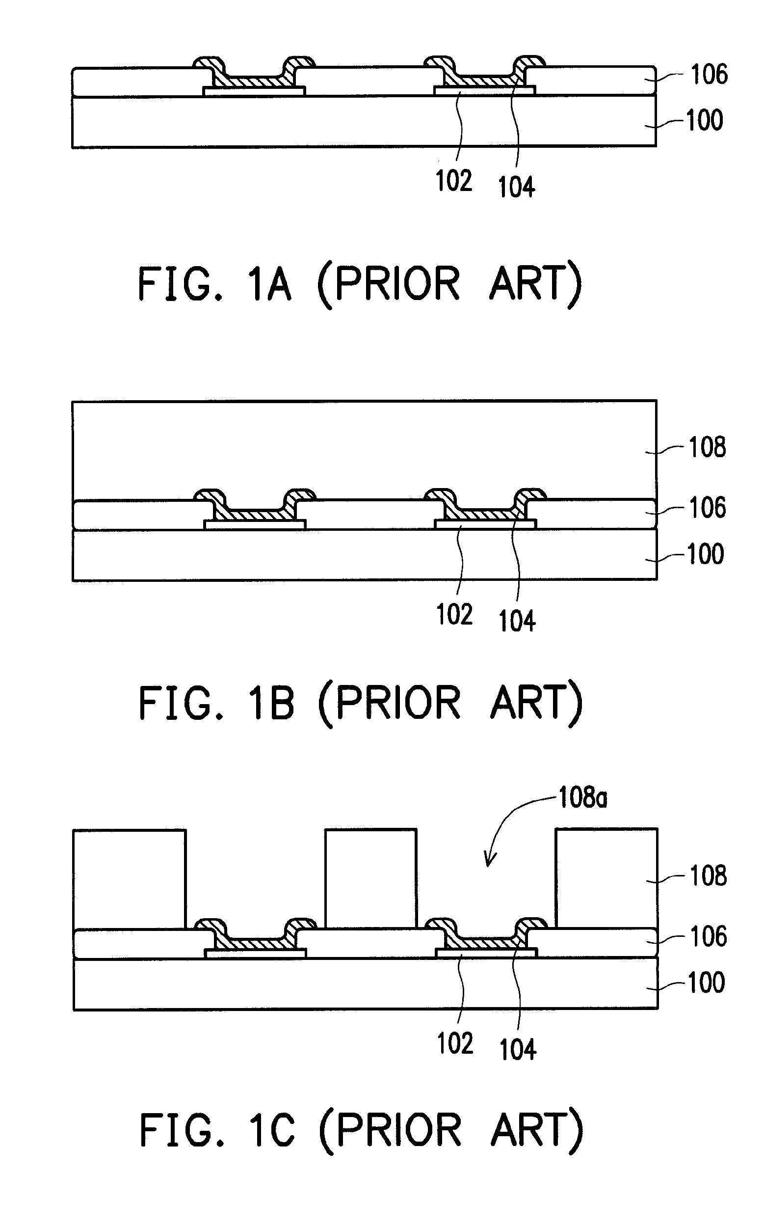
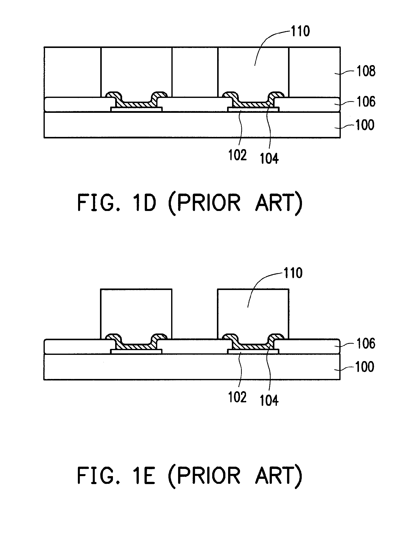
[0027]FIGS. 2A through 2G are schematic cross-sectional views showing a bumping process according to a preferred embodiment of this invention. Referring to FIG. 2A, a wafer 200 having a plurality of pads 202 on the surface of the wafer 200 is provided. The wafer 200 includes a passivation layer 206, which covers the surface of the wafer 200 and exposes the pads 202. In addition, the wafer 200 includes a plurality of UBM layers 204. Each of the UBM layers 204 is deposited on th...
PUM
 Abstract
Description
Claims
Application Information