

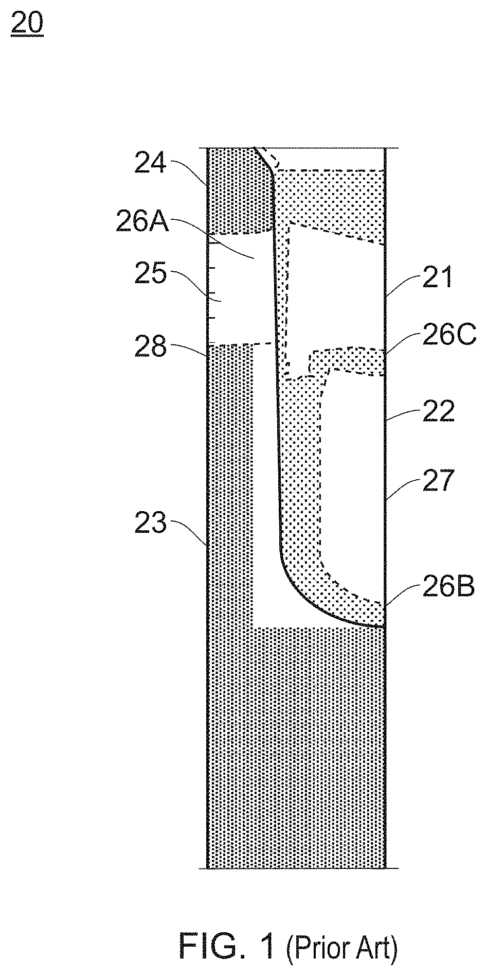
Trench-gate semiconductor device
a semiconductor device and clamping technology, applied in the direction of semiconductor devices, basic electric elements, electrical appliances, etc., can solve the problems of deterioration of leakage and breakdown behavior of these devices, difficulty in properly aligning the second oxide layer, and unreliable breakdown voltage performan
- Summary
- Abstract
- Description
- Claims
- Application Information
AI Technical Summary
Benefits of technology
Problems solved by technology
Method used
Image

Examples
Embodiment Construction
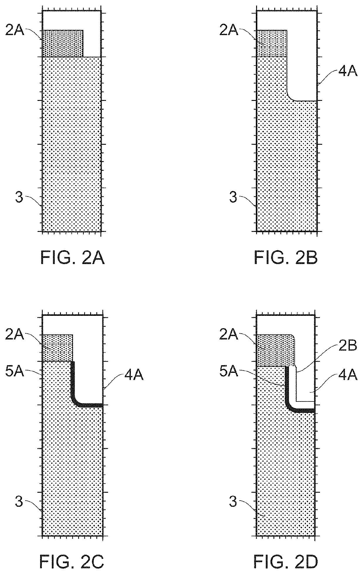
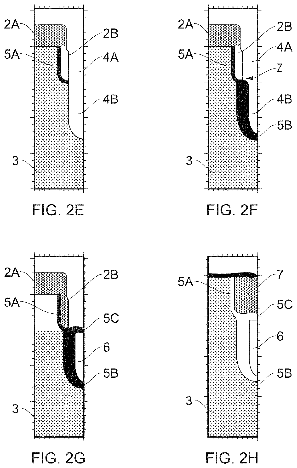
[0046]FIGS. 2A-2H illustrate the process of the first part of manufacturing a unit cell 1 of a trench-gate semiconductor device 100 in which a silicon semiconductor region is used. Remaining process steps will be described with reference to FIG. 3. It is noted that this process can be used to manufacture individual unit cells separately, or to manufacture multiple unit cells simultaneously on a same semiconductor region.
[0047]Referring to FIG. 2A, a first mask layer 2A is deposited and patterned onto a surface of a semiconductor region. For example, first mask layer 2A is provided on top of an epitaxial layer 3 arranged on top of a semiconductor substrate (not shown). First mask layer 2A is patterned such that a portion of the semiconductor region where trench 4A is to be provided is exposed, while a remaining portion of the semiconductor body is covered. For example, silicon nitride or oxide nitride oxide (ONO) can be used for first mask layer 2A.
[0048]Referring to FIG. 2B, first t...
PUM
| Property | Measurement | Unit |
|---|---|---|
| depth | aaaaa | aaaaa |
| depth | aaaaa | aaaaa |
| depth | aaaaa | aaaaa |
Abstract
Description
Claims
Application Information