Multilayer capacitor

a capacitor and multi-layer technology, applied in the field of multi-layer capacitors, can solve the problems of increasing the operating frequency of the central processing unit used for data processing apparatuses, increasing the current consumption of fixed capacitors, and remarkably increasing the current consumption of cpu, so as to reduce the effective inductance and reduce the voltage fluctuations of the cpu power source.

Inactive Publication Date: 2006-02-09
TDK CORPARATION
View PDF5 Cites 21 Cited by
  • Summary
  • Abstract
  • Description
  • Claims
  • Application Information

AI Technical Summary

Benefits of technology

[0017] The present invention has as its object the provision of a multilayer capacitor capable of greatly reducing the effective inductance and reducing the voltage fluctuations in the CPU power source.

Problems solved by technology

In recent years, CPUs (central processing units) used for data processing apparatuses have become higher in operating frequency and remarkably increased in current consumption due to the improvement in processing speeds and higher integration.
It has become extremely difficult to keep voltage fluctuations accompanying current fluctuations to within tolerances of the power sources.
Along with the increasingly higher operating frequencies of today's CPUs, however, the current fluctuations have become faster and larger.
Therefore, it will become impossible to handle the increasingly higher speeds of CPUs in the future.
As a result, in the conventional structure, there is the defect that the total inductance increases and along with this the effective inductance also ends up increasing.
Therefore, it is necessary to reduce this effective inductance.
However, no matter which structure is used, in the past, the total inductance could not be sufficiently reduced and it was not possible to eliminate the defect of the large effective inductance.

Method used


Image

  • Multilayer capacitor
  • Multilayer capacitor
  • Multilayer capacitor

Examples


first embodiment

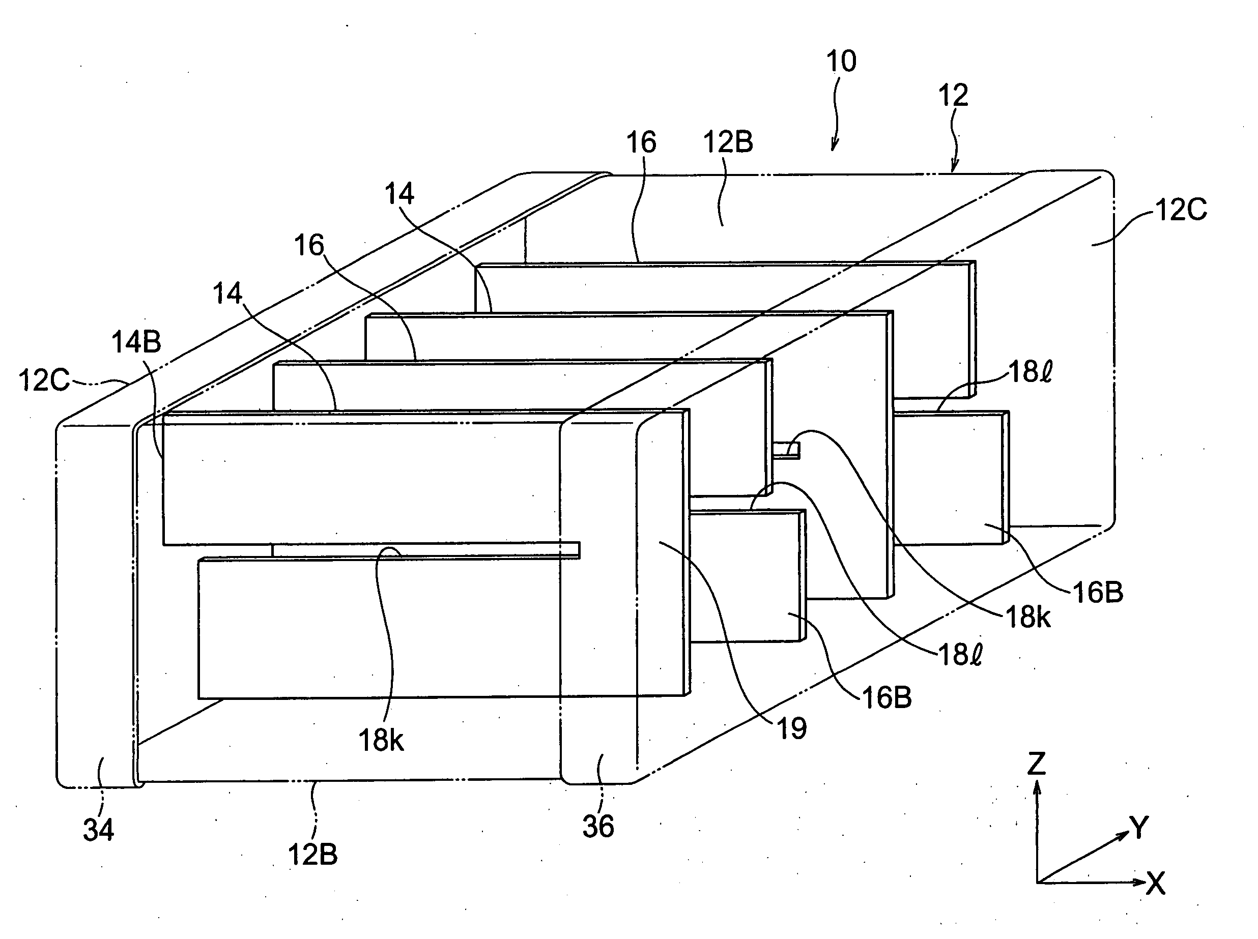
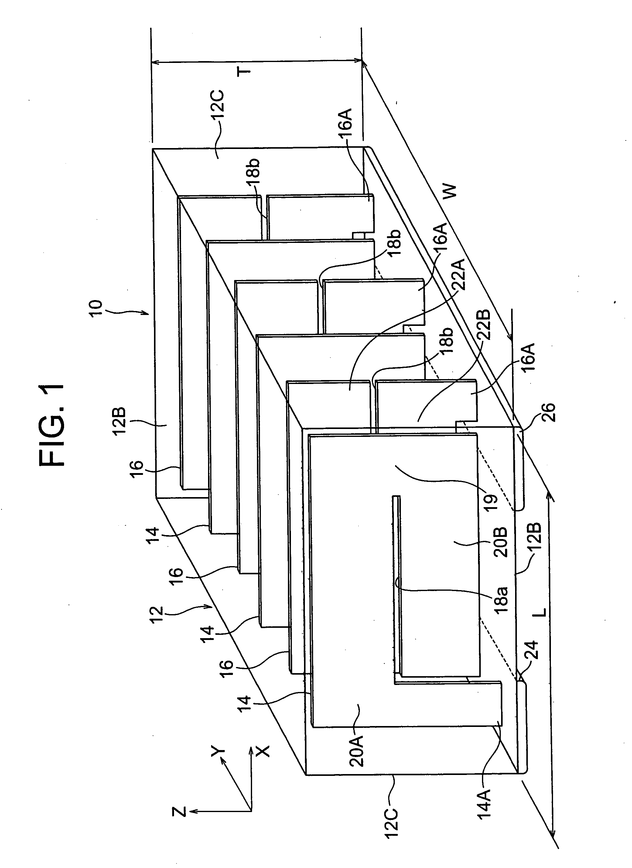
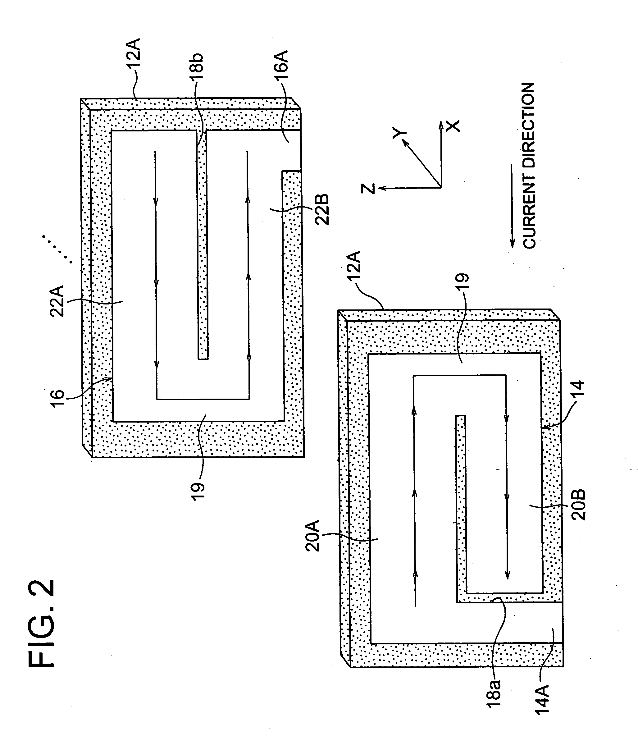
[0065] First, the multilayer capacitor according to a first embodiment of the present invention will be explained. The multilayer ceramic capacitor serving as the multilayer capacitor according to the present invention (hereinafter simply referred to as a “multilayer capacitor”) 10 according to the present embodiment is shown in FIG. 1 to FIG. 3. As shown in these figures, the multilayer capacitor 10 is comprised of, as a main part, a dielectric body 12 comprised of a rectangular parallelepiped shaped sintered body obtained by sintering a stack of a plurality of ceramic green sheets comprising dielectric sheets.

[0066] A planar shaped internal conductor layer (first internal conductor layer) 14 is arranged at a predetermined position inside the dielectric body 12. A similar planar shaped internal conductor layer (second internal conductor layer) 16 is arranged inside the dielectric body 12 at farer side in the stacking direction Y than the internal conductor layer 14 separated by th...

second embodiment

[0092] Next, a multilayer capacitor of a second embodiment of the present invention will be explained based on FIG. 4. Note that members common with members explained in the first embodiment are assigned the same reference numerals and overlapping explanations are omitted.

[0093] The multilayer capacitor of the present embodiment is structured substantially the same as the multilayer capacitor of the first embodiment. However, in the present embodiment, as shown in FIG. 4, two cuts 18c and 18d are formed from the bottom side and top side in an internal conductor layer 14 in parallel and in an inclined direction (with respect to X-axis and Y-axis) in the internal conductor layer 14. Further, an internal conductor layer 16 is formed with two cuts 18e and 18f in parallel and in an inclined direction in a substantially reverse positional relationship from the internal conductor layer 14.

[0094] As a result, an internal conductor layer 14 is formed with three channel parts 20A, 20B, and ...

third embodiment

[0099] Next, a multilayer capacitor of a third embodiment of the present invention will be explained based on FIG. 5. Note that members common with members explained in the first embodiment are assigned the same reference numerals and overlapping explanations are omitted.

[0100] The capacitor of the present embodiment is also structured substantially the same as the capacitor of the first embodiment. However, in the present embodiment, the two cuts 18g and 18h are formed from the bottom side and top side of an internal conductor layer 14 in FIG. 5 in parallel and in the vertical direction (with respect to Z-direction) in the internal conductor layer 14. Further, an internal conductor layer 16 is formed with two cuts 18i and 18j in parallel with each other in the vertical direction in a positional relationship substantially opposite to the internal conductor layer 14.

[0101] That is, while the cut directions differ, in the same way as the second embodiment, two cut parts 18g to 18j a...


PUM

PropertyMeasurementUnit
widthaaaaaaaaaa
currentaaaaaaaaaa
currentaaaaaaaaaa

Abstract

A dielectric body 12 has internal conductor layers 14 arranged in it. At the far sides of the internal conductor layers 14 separated by ceramic layers 12A, internal conductor layers 16 are arranged. A length W of a side of the dielectric body 12 running along a stacking direction Y of the ceramic layers is made longer than the lengths L and T of any other two sides running along directions (X- and Y-directions) intersecting the side running along the stacking direction (Y-direction). The internal conductor layers 14 and 16 are formed with cut parts 18a and 18b, the internal conductor layers 14 are divided into channel parts 20A and 20B across the cut part 18a, and the internal conductor layers 16 are divided into channel parts 22A and 22B across the cut part 18b. These channel parts are connected through uncut ends 19, whereby the current flows in reverse directions. It is therefore possible to greatly reduce the effective inductance of the multilayer capacitor and reduce the voltage fluctuations of the CPU power source.

Description

CROSS-REFERENCE TO RELATED APPLICATION [0001] This is a Division of application Ser. No. 10 / 775,250 filed Feb. 11, 2004. The entire disclosure of the prior application is hereby incorporated by reference herein in its entirety.TECHNICAL FIELD [0002] The present invention relates to a multilayer capacitor capable of greatly reducing the effective inductance, more particularly relates to a multilayer ceramic capacitor capable of reducing the voltage fluctuations of a CPU power source. BACKGROUND ART [0003] In recent years, CPUs (central processing units) used for data processing apparatuses have become higher in operating frequency and remarkably increased in current consumption due to the improvement in processing speeds and higher integration. Along with this, there is a trend toward reduction of the power consumption so as to reduce the operating voltage. Therefore, in power sources for supplying power to CPUs, faster and larger current fluctuations occur. It has become extremely d...

Claims


Application Information

Patent Timeline
Patent Type & Authority Applications(United States)
IPC IPC(8): H01G4/06H01G4/12H01G4/005H01G4/012H01G4/20H01G4/228H01G4/30H02H7/16
CPCH01G4/30H01G4/012G06Q10/02G07B1/00G07B5/00G07F17/42
Inventor TOGASHI, MASAAKIONODERA, SHINYA
Owner TDK CORPARATION
Why Eureka
Try Eureka