
Method for reducing output image noise for thin film field effect transistor liquid crystal display
A technology of thin film field effect and liquid crystal display, applied in the field of reducing output image noise interference, thin film field effect transistor liquid crystal display to reduce output image noise, can solve the problem that noise is difficult to improve, to improve noise problem, reduce vibration, increase cost effect
- Summary
- Abstract
- Description
- Claims
- Application Information
AI Technical Summary
Problems solved by technology
Method used
Image

Examples
Embodiment 1
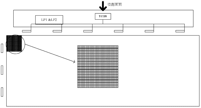
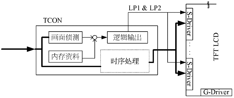
[0042] The present invention detects the input image image through the detection image device, that is, the pulse controller (TCON), and the TCON controls the LP1 & LP2 pins of the SD respectively according to the different image images, so as to reduce the drastic change of the Vout voltage caused by the instant liquid crystal voltage pumping.
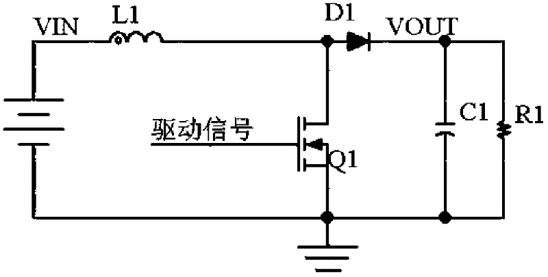
[0043] There is a Boost circuit inside the panel Figure II As shown, the Vout voltage in the Boost circuit supplies the driving liquid crystal voltage. Generally speaking, C1 uses a multi-layer stacked ceramic capacitor (MLCC) as a voltage stabilizing capacitor. Due to the dynamic adjustment of the drive capability of the panel SD, the drastic fluctuation of the Vout voltage is reduced, and the vibration of the MLCC is also reduced, and the noise problem can be improved.
[0044] The SD drive capacity is divided into the following table, and the SD thrust is controlled by the two pins (LP1&LP2),
[0045] LP1 LP2 Analog...
PUM
 Abstract
Description
Claims
Application Information