Display device

Active Publication Date: 2011-06-30
SEMICON ENERGY LAB CO LTD
View PDF20 Cites 7 Cited by
  • Summary
  • Abstract
  • Description
  • Claims
  • Application Information

AI Technical Summary

Benefits of technology

[0014]Multi-gray scale display can be realized by reducing voltage fluctuation of a pixel. Further, display device having high-quality display can b

Problems solved by technology

However, it has been difficult to realize multi-gray scale display in these d

Method used


Image

  • Display device
  • Display device
  • Display device

Examples


Example

Embodiment 1

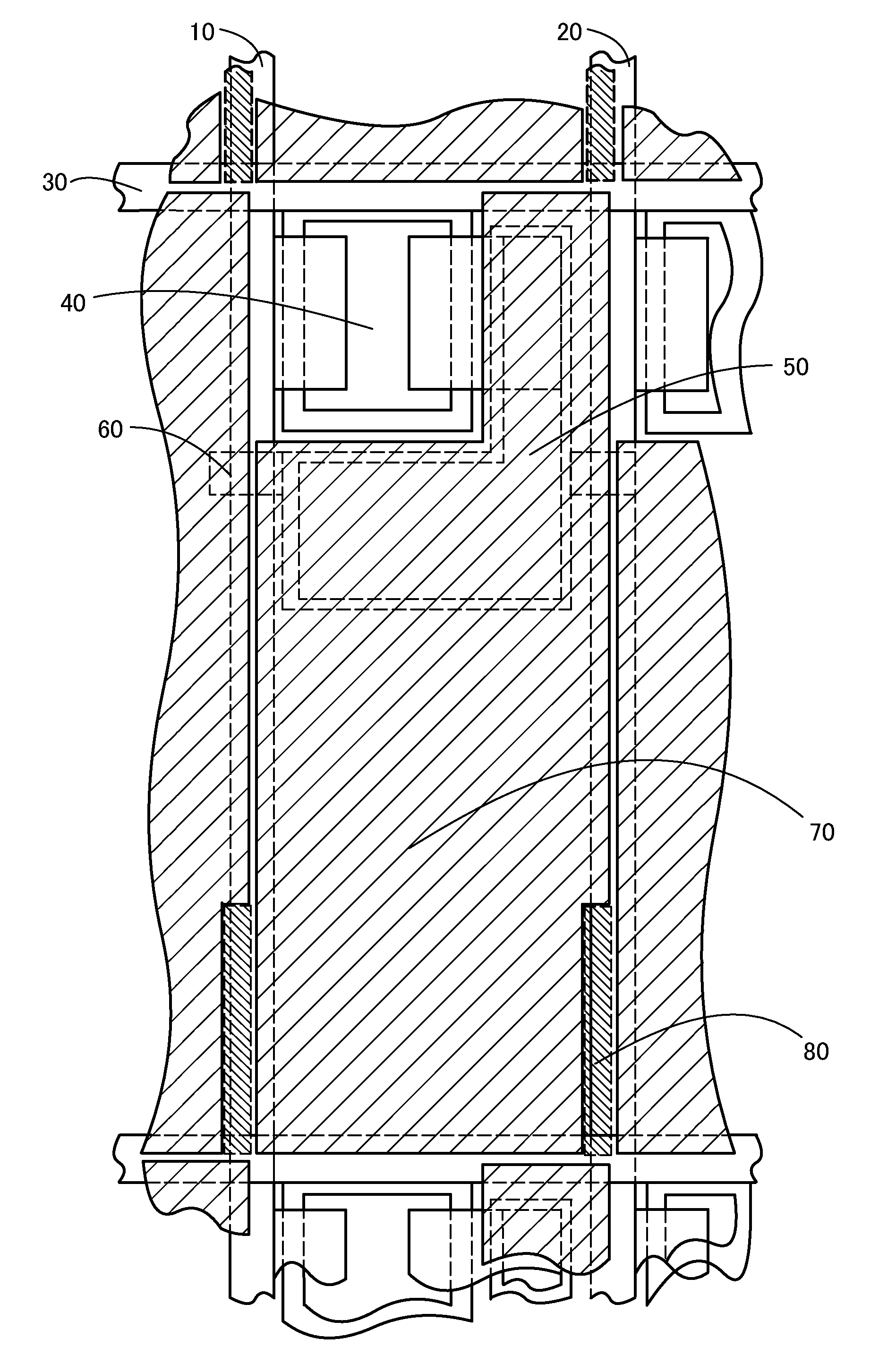
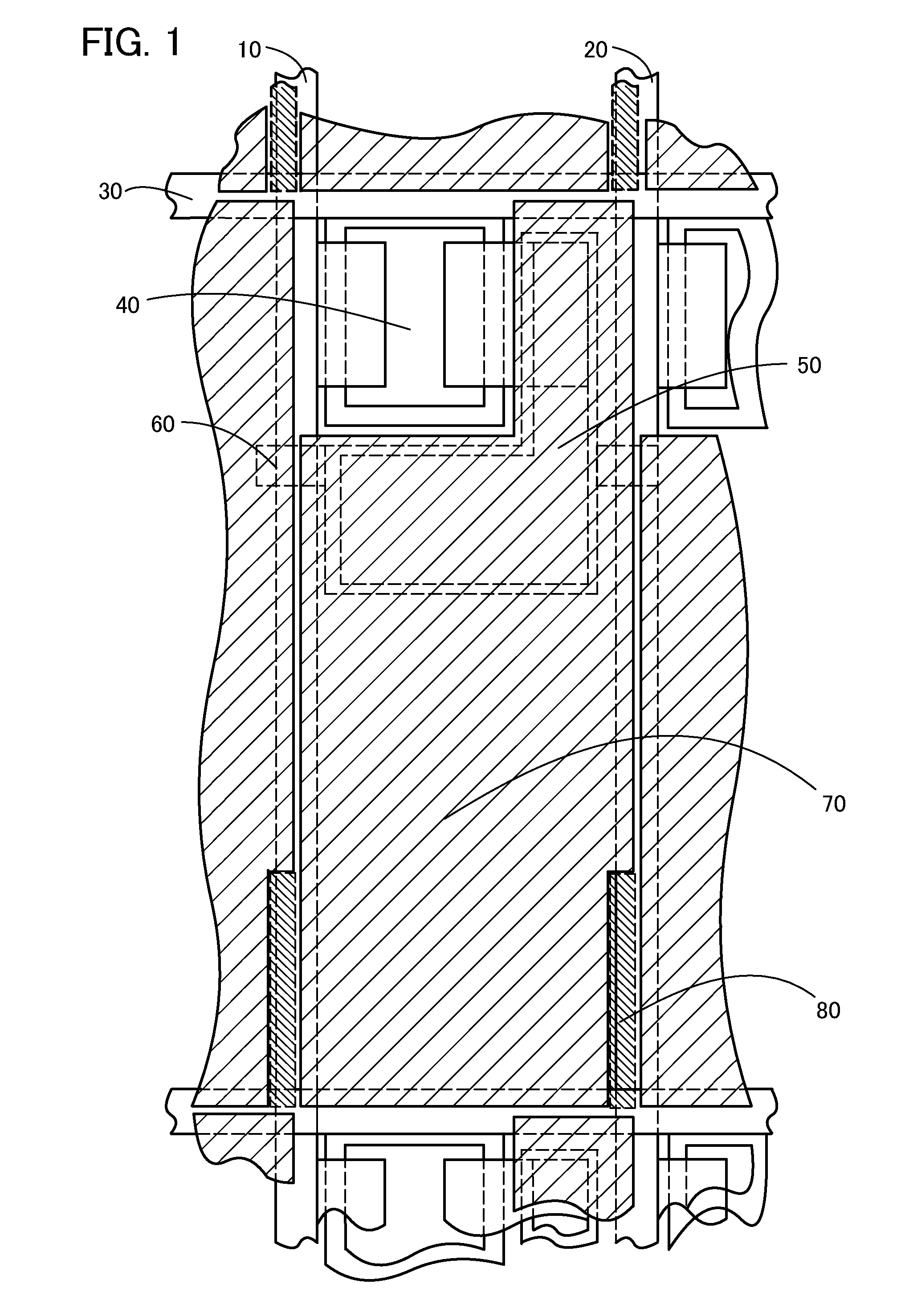
[0028]FIG. 1 is a plan view illustrating a structural example of a pixel in a display device. The display device includes source signal lines 10 and 20, a gate signal line 30, a transistor 40, a storage capacitor 50, a capacitor line 60, and a pixel electrode 70.

[0029]In the display device, a plurality of signal lines including the signal lines 10 and 20 are provided. In addition, a plurality of gate signal lines including the gate signal line 30 are provided in matrix with respect to the source signal lines.

[0030]The transistor 40 serving as a switching element is provided near an intersection portion of the source signal line 10 and the gate signal line 30. The storage capacitor 50 and the capacitor line 60 are provided adjacent to the transistor 40.

[0031]The pixel electrode 70 is formed so that the edge portions thereof overlap with the edge portions of a pair of the adjacent source signal lines 10 and 20 and the edge portions of a pair of the adjacent gate signal lin...

Example

Embodiment 2

[0064]In this embodiment, an example of a structure of a transistor including an intrinsic or substantially intrinsic oxide semiconductor and an example of a manufacturing method thereof will be described.

[0065]An example of a plan structure and an example of a cross-sectional structure of a transistor are respectively illustrated in FIGS. 6A and 6B. FIG. 6A is a plan view of a top-gate transistor, and FIG. 6B is a cross-sectional view taken along line C1-C2 of FIG. 6A.

[0066]A transistor 410 includes, over a substrate 400, an insulating layer 407, an oxide semiconductor layer 412, a first electrode (one of a source electrode and a drain electrode) 415a, a second electrode (the other of the source electrode and the drain electrode) 415b, a gate insulating layer 402, and a gate electrode 411. A first wiring layer 414a and a second wiring layer 414b are provided in contact with and electrically connected to the first electrode 415a and the second electrode 415b, respectivel...

Example

Embodiment 3

[0126]In this embodiment, another example of a structure of a transistor including an intrinsic or substantially intrinsic oxide semiconductor and another example of a manufacturing method thereof will be described.

[0127]FIGS. 8A to 8E illustrate an example of a structure and a manufacturing method of a transistor. A transistor 390 illustrated in FIG. 8E is one type of a bottom gate structure and is also referred to as an inverted staggered transistor. The transistor 390 can be used for the transistor described in Embodiment 1, for example. Note that although the transistor 390 has a single-gate structure, the present invention is not limited to this structure. The transistor may have a multi-gate structure which includes a plurality of gate electrodes and a plurality of channel formation regions.

[0128]A manufacturing method of the transistor 390 over a substrate 394 will be described below with reference to FIGS. 8A to 8E.

[0129]First, a conductive film is formed over th...


PUM


Abstract

To provide a display device which can realize multi-gray scale display by reducing voltage fluctuation of a pixel, a display device includes a plurality of source signal lines, a plurality of gate signal lines which is provided so as to intersect with the source signal lines, and a pixel electrode to which a signal voltage of the source signal line is applied through a transistor including an oxide semiconductor, which is provided near an intersection portion of the source signal line and the gate signal line; in which in the pixel electrode which is provided between a pair of the adjacent source signal lines, edge portions thereof overlap with edge portions of the source signal lines and an overlapped area with one of the source signal lines is substantially equal to an overlapped area with the other source signal line.

Description

TECHNICAL FIELD[0001]The technical field of the present invention relates to a display device, in particular, a display device which can realize multi-gray scale display.BACKGROUND ART[0002]Display devices which are driven with transistors including amorphous silicon or polysilicon have been mainly used. However, it has been difficult to realize multi-gray scale display in these display devices due to the effect of the off-state current of the transistors.[0003]As an example of a pixel in a display device, FIG. 12 illustrates a pixel including a transistor 100, a liquid crystal element 110, and a storage capacitor 120. The transistor 100 is an amorphous silicon transistor or a polysilicon transistor. In each pixel, image data is written into the liquid crystal element 110 and the storage capacitor 120 from the transistor 100, so that the liquid crystal element 110 is provided with an electric filed; accordingly, an image can be displayed.[0004]However, the electric charges accumulat...

Claims


Application Information

Patent Timeline
IPC IPC(8): G09G3/36
CPCG02F1/136286H01L21/02554H01L21/02414G02F2001/13606G02F1/13606H01L21/02565H01L21/02631
Inventor KOYAMA, JUN
Owner SEMICON ENERGY LAB CO LTD
Why Eureka
Try Eureka