
Printed circuit board including embedded capacitor having high dielectric constant and method of fabricating same
a technology of embedded capacitors and printed circuit boards, which is applied in the direction of fixed capacitors, fixed capacitor details, thin/thick film capacitors, etc., can solve the problems of reducing the electric performance of goods, not yet achieving standardization of the above methods, and not yet activating the market for pcbs including embedded capacitors. , to achieve the effect of reducing material costs, reducing costs, and ensuring ease of production
- Summary
- Abstract
- Description
- Claims
- Application Information
AI Technical Summary
Benefits of technology
Problems solved by technology
Method used
Image

Examples
first embodiment
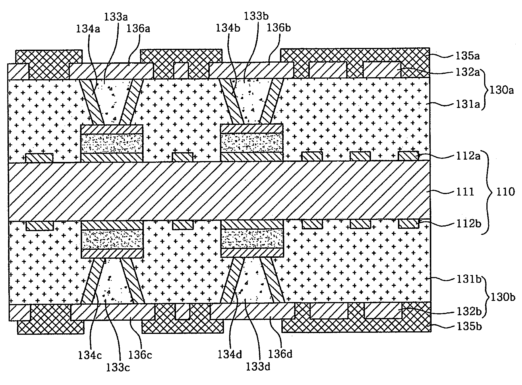
[0061]FIG. 4a is a sectional view of a PCB including embedded capacitors each having a high dielectric constant according to the present invention.
[0062] Referring to FIG. 4a, circuit layers 112a, 112b including patterned copper foils are formed on both sides of an insulating layer 111 constituting a core layer 110.
[0063] At this time, lower electrodes 121a, 121b, 121c, 121d of the embedded capacitors 120a, 120b, 120c, 120d are formed in the circuit layers 112a, 112b.
[0064] The embedded capacitors 120a, 120b, 120c, 120d include the lower electrodes 121a, 121b, 121c, 121d formed in the circuit layers 112a, 112b, insulating layers 122a, 122b, 122c, 122d made of ceramic materials and laminated on the lower electrodes 121a, 121b, 121c, 121d, and upper electrodes 123a, 123b, 123c, 123d laminated on the insulating layers 122a, 122b, 122c, 122d.
[0065] The embedded capacitors 120a, 120b, 120c, 120d may also include an adhesive metal layer, which consists of an adhesive metal such as Cr, ...
second embodiment
[0068]FIG. 4b is a sectional view of a PCB including embedded capacitors each having a high dielectric constant according to the present invention.
[0069] Referring to FIG. 4b, circuit layers 112a, 112b including patterned copper foils are formed on both sides of an insulating layer 111 constituting a core layer 110. Insulators 113a, 113b such as resins are packed into a portion of the circuit layers 112a, 112b on which circuit patterns are not formed.
[0070] At this time, lower electrodes 121a, 121b, 121c, 121d of the embedded capacitors 120a, 120b, 120c, 120d are formed in the circuit layers 112a, 112b.
[0071] Insulating layers 122a, 122b made of ceramic materials are laminated on the circuit layers 112a, 112b.
[0072] Circuit layers 125a, 125b on which circuit patterns are formed are formed on the insulating layers 122a, 122b, and upper electrodes 123a, 123b, 123c, 123d that correspond to the lower electrodes 121a, 121b, 121c, 121d are formed on the circuit layers 125a, 125b.
[0073...
third embodiment
[0121]FIGS. 8a to 8f illustrate the production of a PCB including embedded capacitors each having a high dielectric constant according to the present invention.
[0122] As shown in FIG. 8a, a copper clad laminate 510, which includes an insulating layer 511 and copper foils 512a, 512b formed on both sides of the insulating layer 511, is provided to fabricate a PCB including embedded capacitors each having a high dielectric constant according to the third embodiment of the present invention.
[0123] As shown in FIG. 8b, a wiring pattern is formed on the copper foils 512a, 512b according to a photolithography process. At this time, lower electrodes 521a-521d of embedded capacitors 520a-520d are formed simultaneously.
[0124] As shown in FIG. 8c, resins 515a, 515b are formed on the copper clad laminate 510, on which circuits are formed, according to a vacuum printing process. Flattening the resins 515a, 515b increases their interfacial adhesion to a ceramic material.
[0125] Referring to FIG...
PUM
| Property | Measurement | Unit |
|---|---|---|
| roughness | aaaaa | aaaaa |
| dielectric constant | aaaaa | aaaaa |
| thickness | aaaaa | aaaaa |
Abstract
Description
Claims
Application Information