Printed circuit board including embedded capacitor having high dielectric constant and method of fabricating same

a technology of embedded capacitors and printed circuit boards, which is applied in the direction of fixed capacitors, printed circuit non-printed electric components associations, thin/thick film capacitors, etc., can solve the problems of reducing the electric performance of goods, not yet achieving standardization of the above methods, and not yet activating the market for pcbs including embedded capacitors. , to achieve the effect of reducing material costs, reducing costs, and ensuring ease of production

Inactive Publication Date: 2007-06-28
SAMSUNG ELECTRO MECHANICS CO LTD
View PDF8 Cites 16 Cited by
  • Summary
  • Abstract
  • Description
  • Claims
  • Application Information

AI Technical Summary

Benefits of technology

[0046] Another object of the present invention is to provide a PCB including embedded capacitors each having a high dielectric constant and a method of fabricating the same, in which only a desired part is made of a ceramic material to form a dielectric thin film (or thick film), thereby creating the embedded capacitors. Accordingly, a loss of costly raw materials is reduced and unnecessary processes, such as a process of etching a dielectric, may be omitted, consequently, material costs are reduced and ease of production is assured.

Problems solved by technology

However, a market for PCBs including embedded capacitors is not yet activated.
Accordingly, standardization of the above methods has not been achieved yet, but commercialization of the methods is under development.
In conventional technologies, a long connection length between devices at a high frequency brings about occurrence of an electric parasitic load, thereby reducing the electric performances of goods.
Additionally, the number of connections increases due to a solder, causing poor reliability of goods.
Furthermore, in the third conventional technology, capacitance is low due to a low dielectric constant of an embedded capacitor layer.
Accordingly, there are many limits to the realization of the conventional embedded capacitor.
However, these procedures result in increased production costs because the formation of upper and lower electrodes, and exposure and etching processes for patterning the insulating layer are additionally carried out.

Method used


Image

  • Printed circuit board including embedded capacitor having high dielectric constant and method of fabricating same
  • Printed circuit board including embedded capacitor having high dielectric constant and method of fabricating same
  • Printed circuit board including embedded capacitor having high dielectric constant and method of fabricating same

Examples


first embodiment

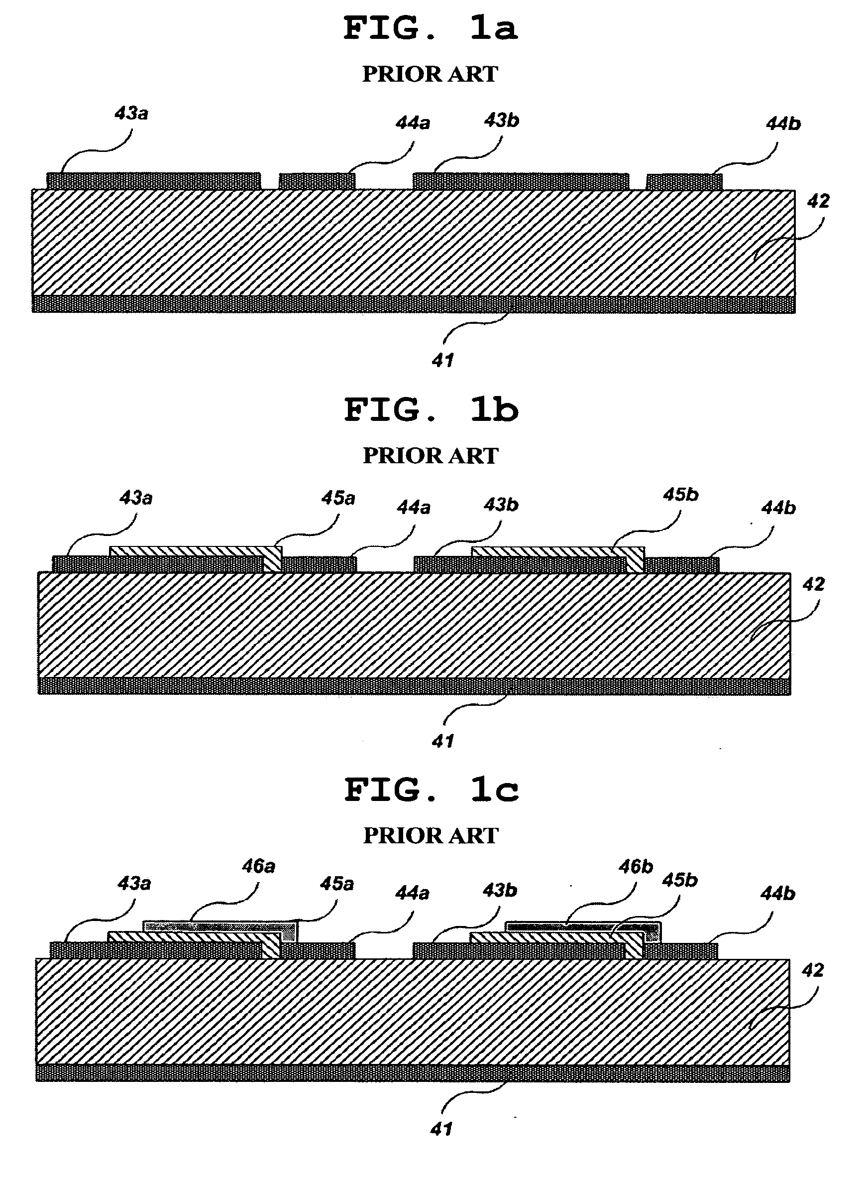
[0061]FIG. 4a is a sectional view of a PCB including embedded capacitors each having a high dielectric constant according to the present invention.

[0062] Referring to FIG. 4a, circuit layers 112a, 112b including patterned copper foils are formed on both sides of an insulating layer 111 constituting a core layer 110.

[0063] At this time, lower electrodes 121a, 121b, 121c, 121d of the embedded capacitors 120a, 120b, 120c, 120d are formed in the circuit layers 112a, 112b.

[0064] The embedded capacitors 120a, 120b, 120c, 120d include the lower electrodes 121a, 121b, 121c, 121d formed in the circuit layers 112a, 112b, insulating layers 122a, 122b, 122c, 122d made of ceramic materials and laminated on the lower electrodes 121a, 121b, 121c, 121d, and upper electrodes 123a, 123b, 123c, 123d laminated on the insulating layers 122a, 122b, 122c, 122d.

[0065] The embedded capacitors 120a, 120b, 120c, 120d may also include an adhesive metal layer, which consists of an adhesive metal such as Cr, ...

second embodiment

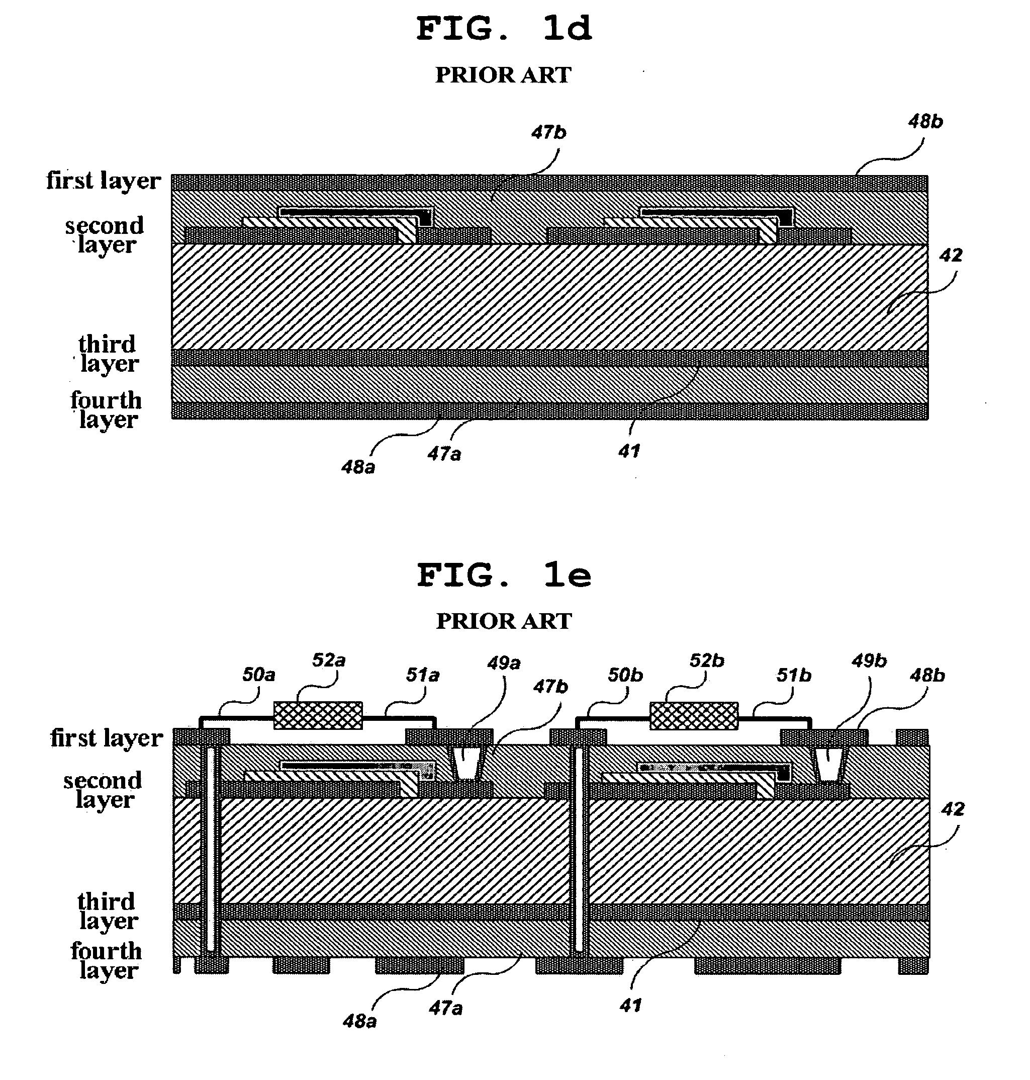
[0068]FIG. 4b is a sectional view of a PCB including embedded capacitors each having a high dielectric constant according to the present invention.

[0069] Referring to FIG. 4b, circuit layers 112a, 112b including patterned copper foils are formed on both sides of an insulating layer 111 constituting a core layer 110. Insulators 113a, 113b such as resins are packed into a portion of the circuit layers 112a, 112b on which circuit patterns are not formed.

[0070] At this time, lower electrodes 121a, 121b, 121c, 121d of the embedded capacitors 120a, 120b, 120c, 120d are formed in the circuit layers 112a, 112b.

[0071] Insulating layers 122a, 122b made of ceramic materials are laminated on the circuit layers 112a, 112b.

[0072] Circuit layers 125a, 125b on which circuit patterns are formed are formed on the insulating layers 122a, 122b, and upper electrodes 123a, 123b, 123c, 123d that correspond to the lower electrodes 121a, 121b, 121c, 121d are formed on the circuit layers 125a, 125b.

[0073...

third embodiment

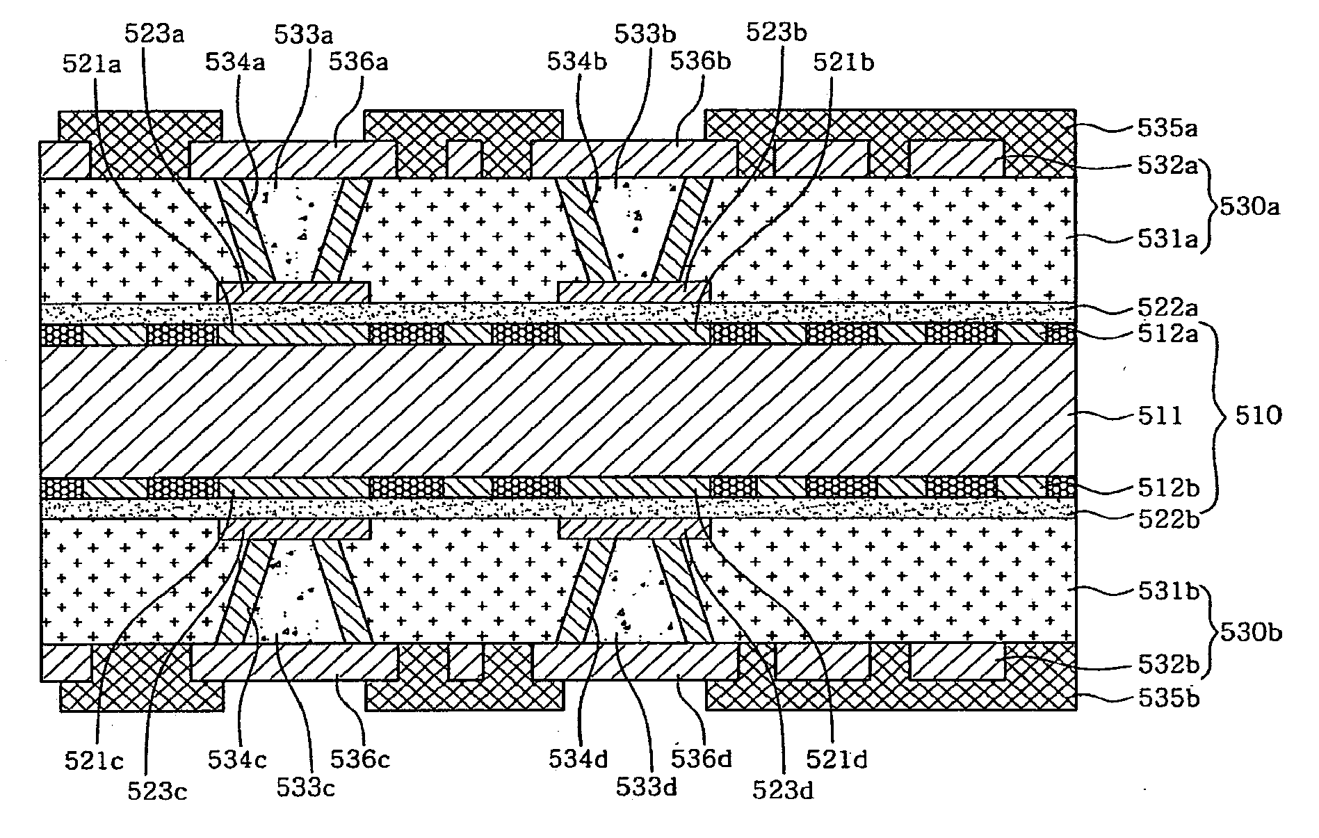
[0121]FIGS. 8a to 8f illustrate the production of a PCB including embedded capacitors each having a high dielectric constant according to the present invention.

[0122] As shown in FIG. 8a, a copper clad laminate 510, which includes an insulating layer 511 and copper foils 512a, 512b formed on both sides of the insulating layer 511, is provided to fabricate a PCB including embedded capacitors each having a high dielectric constant according to the third embodiment of the present invention.

[0123] As shown in FIG. 8b, a wiring pattern is formed on the copper foils 512a, 512b according to a photolithography process. At this time, lower electrodes 521a-521d of embedded capacitors 520a-520d are formed simultaneously.

[0124] As shown in FIG. 8c, resins 515a, 515b are formed on the copper clad laminate 510, on which circuits are formed, according to a vacuum printing process. Flattening the resins 515a, 515b increases their interfacial adhesion to a ceramic material.

[0125] Referring to FIG...


PUM

PropertyMeasurementUnit
roughnessaaaaaaaaaa
dielectric constantaaaaaaaaaa
thicknessaaaaaaaaaa

Abstract

Disclosed is a PCB including embedded capacitors and a method of fabricating the same. A dielectric layer is formed using a ceramic material having a high capacitance, thereby assuring that the capacitors each have a high dielectric constant corresponding to the capacitance of a decoupling chip capacitor.

Description

INCORPORATION BY REFERENCE [0001] The present application claims priority under 35 U.S.C. §119 to Korean Patent Application No. 2004-67487 filed on Aug. 26, 2004. The content of the application is incorporated herein by reference in its entirety. BACKGROUND OF THE INVENTION [0002] 1. Field of the Invention [0003] The present invention relates, in general, to a printed circuit board (PCB) including embedded capacitors and a method of fabricating the same and, more particularly, to a PCB including embedded capacitors, in which a dielectric layer is formed using a ceramic material having a high capacitance, thereby assuring that the capacitors each have a high dielectric constant corresponding to the capacitance of a decoupling chip capacitor, and a method of fabricating the same. [0004] 2. Description of the Prior Art [0005] Typically, discrete chip resistors or discrete chip capacitors have been frequently mounted on most printed circuit boards (PCB), but, recently, PCBs are developi...

Claims


Application Information

Patent Timeline
Patent Type & Authority Applications(United States)
IPC IPC(8): H04R17/00
CPCH01G4/1209Y10T29/42H01G4/248H01G4/33H05K1/162H05K3/4652H05K2201/0175H05K2201/0179H05K2201/0195H05K2201/09509H05K2201/09763H05K2201/09881H05K2203/0568H05K2203/1366H01G4/1218H05K1/16
Inventor AHN, JIN-YONGRYU, CHANG-SUPCHO, SUK-HYEONLEE, SEOK-KYUHONG, JONG-KUKJUN, HO-SIK
Owner SAMSUNG ELECTRO MECHANICS CO LTD
Why Eureka
Try Eureka