

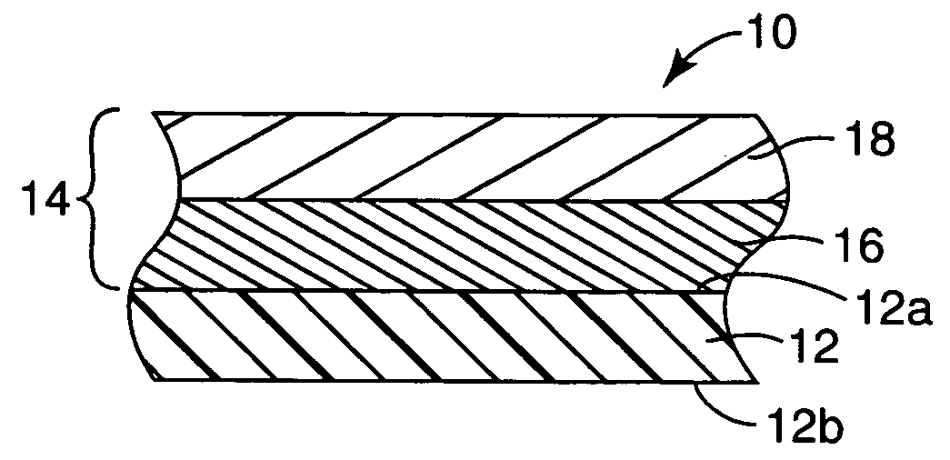
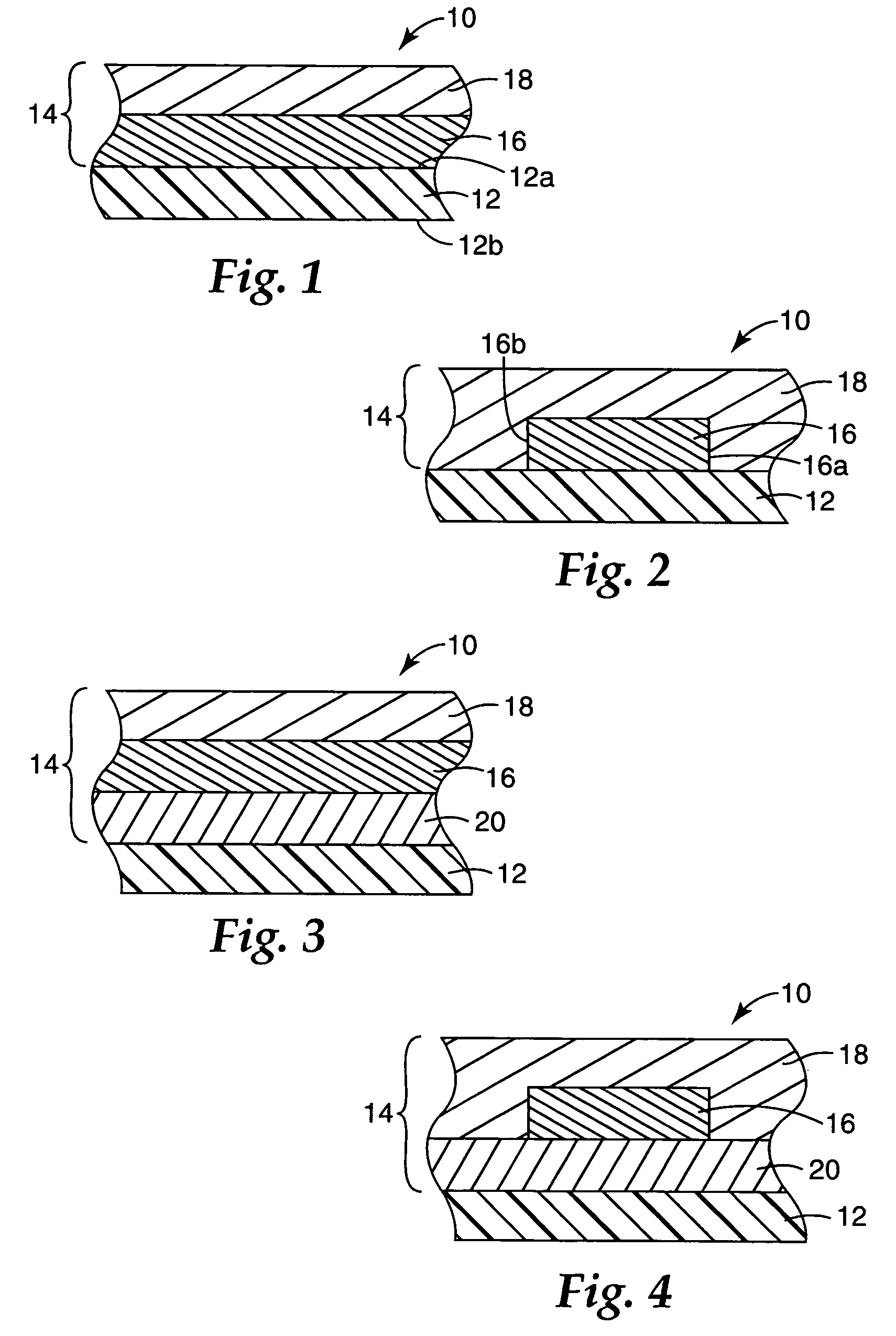
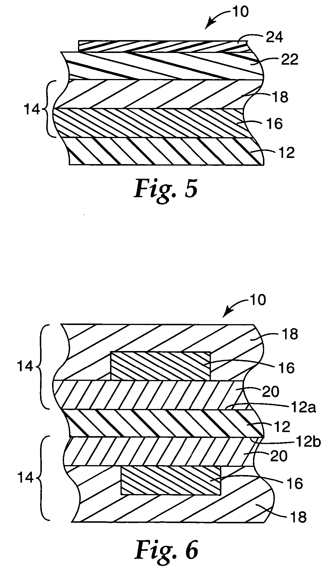
Protected polymeric film
a polymeric film and film technology, applied in the field of protected polymeric films, can solve the problems of reduced output or premature failure of organic electroluminescent devices, limited success so far, etc., and achieve the effect of reducing the inherent, but potentially undesirable, tendency of polymeric films to transmit moisture and reducing the transmission of moistur
- Summary
- Abstract
- Description
- Claims
- Application Information
AI Technical Summary
Benefits of technology
Problems solved by technology
Method used
Image

Examples
example 1
[0047] An OLED device incorporating a protected polymeric film according to the invention was prepared in Example 1. A UV-curable solution was prepared by combining 80 grams Ebecryl 629, 20 grams SR399, and 2 grams Irgacurel 84 that had been dissolved in 1000 grams of MEK. The resulting solution was coated onto a roll of 6.5 inch wide HSPE 100 PET film substrate using a CAG 150 microgravure coater operating at 20 ft / min. The coating was subsequently in-line dried at 70° C. and then cured under a nitrogen atmosphere with a Fusion D UV Lamp operating at 100% power. This resulted in a transparent PET film substrate having an approximately 0.7 μm thick transparent coating thereon.
[0048] A polymer web mask commercially available from 3M Company under the trade designation Scotchpak 1220 was die cut and then thermally laminated to the coated surface of the PET film substrate using a roll-to-roll laminator. An approximately 35 nm thick layer of ITO, followed by an approximately 10 nm thic...
example 2
[0061] An OLED device incorporating a protected polymeric film according to the invention was prepared in Example 2. Additional samples of OLED Device A from Example 1 were prepared and the copper foil was edge sealed using a thin bead of epoxy (Araldite 2014 available from Huntsman LLC, Advanced Materials Division, Vantico, East Lansing, Mich.). The epoxy was allowed to cure to hardness over 12 hours in a N2 atmosphere at room temperature. For convenience, this is referred to as “OLED Device B.”
[0062] An inorganic barrier layer was then prepared according to the following procedure. A UV-curable polymer solution was prepared by combining 2.25 grams UVI-6974 with 42.75 grams EHPE3150 in 405 grams MEK. The resulting solution was coated onto a 6.5 inch wide, 100 micron thick fluorine polyester film commercially available from Ferrania Imaging Technologies, Italy, under the trade designation Arylite using a CAG 150 microgravure coater operating at a speed of 15 ft / min. The coating was ...
PUM
| Property | Measurement | Unit |
|---|---|---|
| Acoustic impedance | aaaaa | aaaaa |
| Acoustic impedance | aaaaa | aaaaa |
| Transmission | aaaaa | aaaaa |
Abstract
Description
Claims
Application Information