Display device
a display device and display screen technology, applied in the field of display devices, can solve the problems of strict inspection of wiring defects such as short-circuit between the wiring lines and the breakage of each wiring line, and achieve the effect of suppressing the drop of manufacturing yield and stably conducting inspection of quality
- Summary
- Abstract
- Description
- Claims
- Application Information
AI Technical Summary
Benefits of technology
Problems solved by technology
Method used
Image

Examples
first embodiment
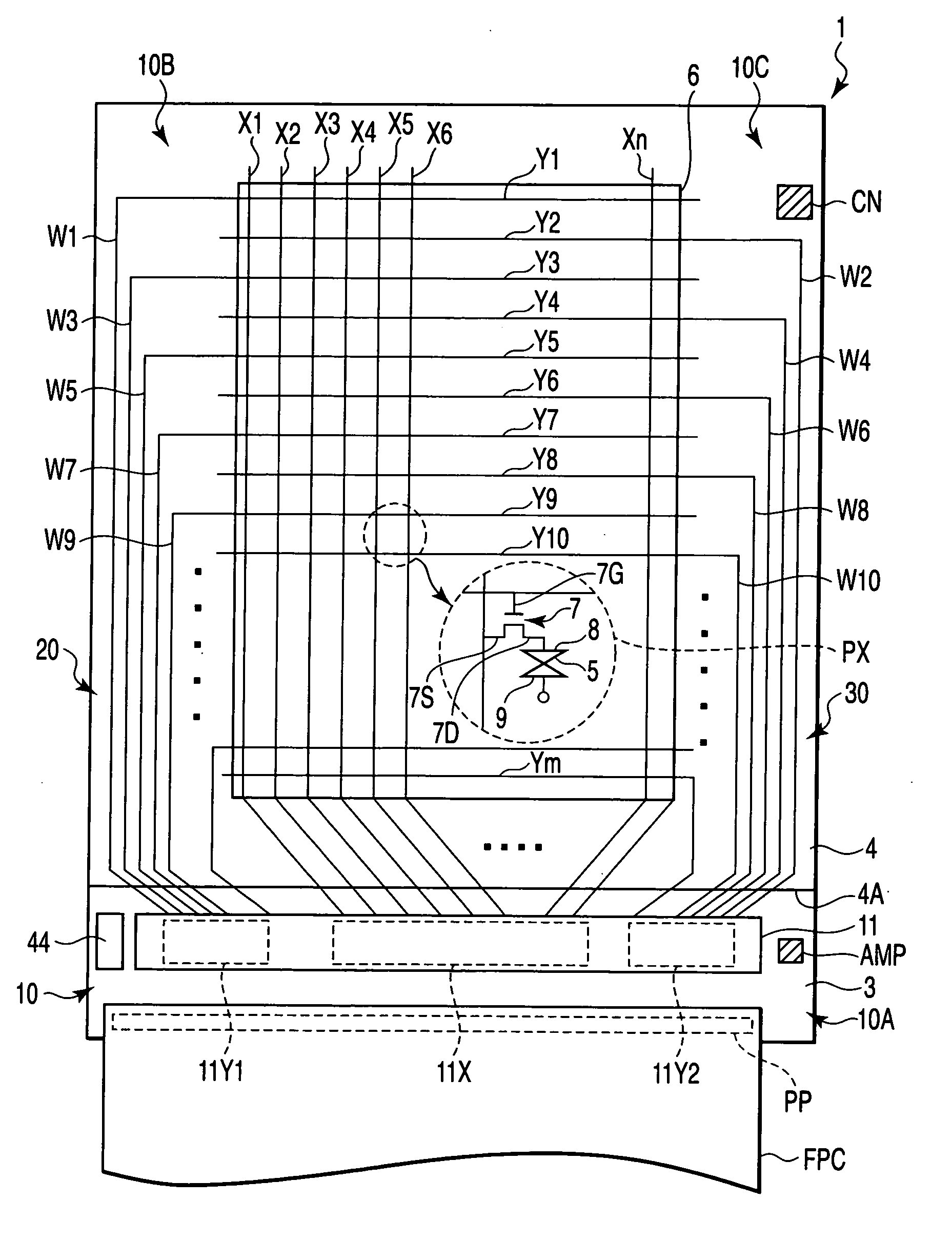
[0087] As is shown in FIG. 1, a liquid crystal display device, which is an example of a display device according to a first embodiment, includes a substantially rectangular, planar liquid crystal display panel 1. The liquid crystal display panel 1 is constituted of a pair of substrates, that is, an array substrate 3 and a counter-substrate 4, and a liquid crystal layer 5 that is interposed as an optical modulation layer between the pair of substrates. The liquid crystal display panel 1 includes a substantially rectangular effective display section 6 that displays an image. The effective display section 6 is composed of a plurality of display pixels PX that are arranged in a matrix.
[0088] The array substrate 3 includes, in the effective display section 6, a plurality of scan lines Y (1, 2, 3, . . . , m) that extend in a row direction of the display pixels PX, a plurality of signal lines X (1, 2, 3, . . . , n) that extend in a column direction of the display pixels PX, switch element...
example 1
Conductive Layer-Inspection Control Wiring Line; Disposed in the Same Layer
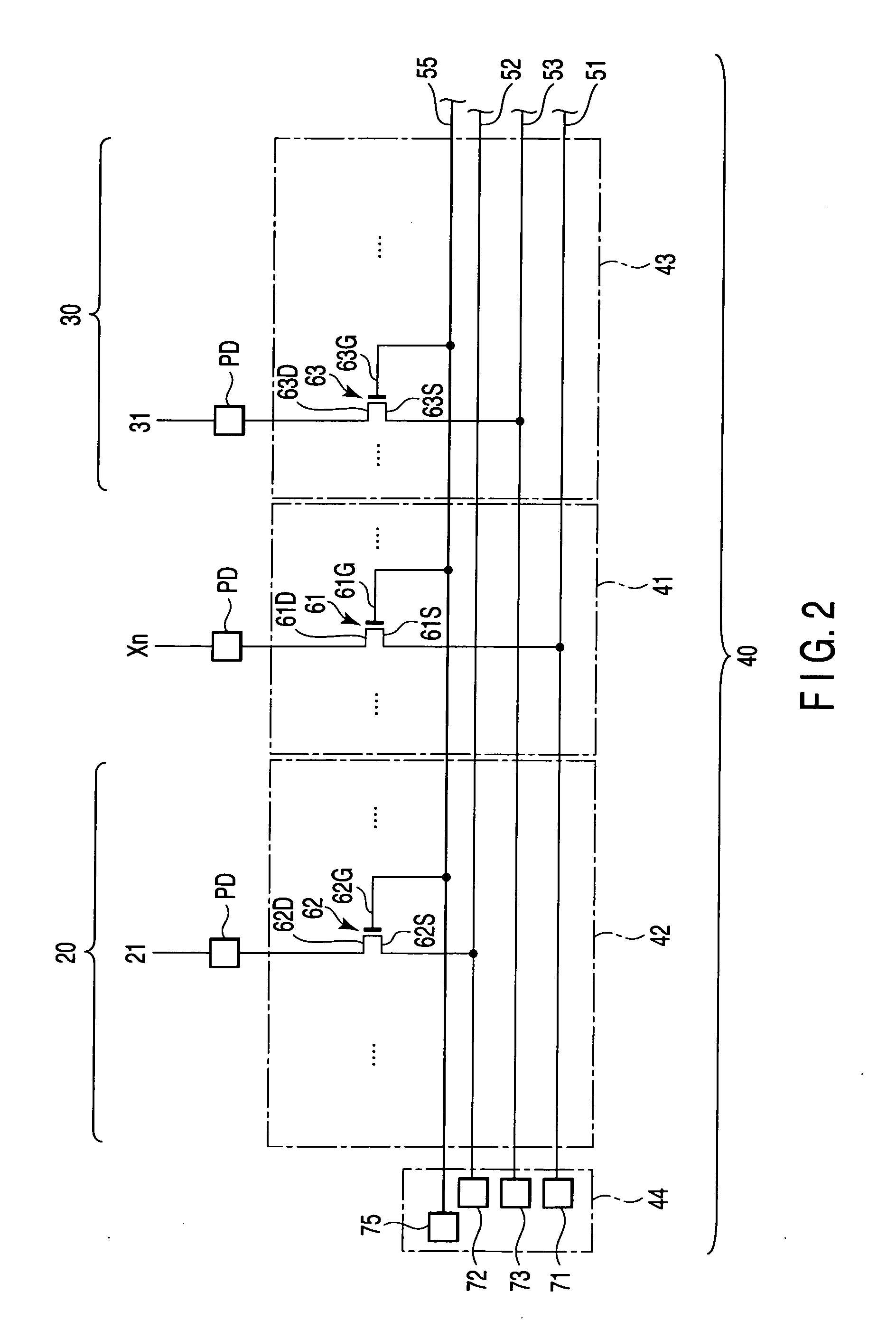
[0156] In Example 1, a constitution example will be described in which discharge is induced in an end portion 55E of an inspection control wiring line 55. As shown in FIGS. 12A and 12B, the end portion 55E of the inspection control wiring line 55 is disposed in such a manner as to face a conductive layer 90 at a predetermined interval in the same layer as that of the inspection control wiring line 55 integral with a gate electrode 63G of a switch element 63. The end portion 55E of the inspection control wiring line 55 facing the conductive layer 90 has a salient portion C protruding toward the conductive layer 90. A discharge inducing portion 90A of the conductive layer 90 facing the inspection control wiring line 55 has a salient portion C protruding toward the inspection control wiring line 55. That is, the inspection control wiring line 55 and the conductive layer 90 are disposed in such a manner that ver...
example 2
Conductive Layer-Inspection Control Wiring Line; Disposed in Different Layers
[0158] In Example 2, a constitution example will be described in which discharge in an end portion 55E of an inspection control wiring line 55 is induced. As shown in FIGS. 13A and 13B, a conductive layer 90 is disposed in a lower layer of an insulating layer 100. The inspection control wiring line 55 integral with a gate electrode 63G of a switch element 63 is disposed in an upper layer of the insulating layer 100. The end portion 55E facing the conductive layer 90 of the inspection control wiring line 55 has a salient portion C that protrudes toward the conductive layer 90. A discharge inducing portion 90A that faces the inspection control wiring line 55 of the conductive layer 90 has a salient portion C that protrudes toward the inspection control wiring line 55. That is, the end portion 55E of the inspection control wiring line 55 is disposed in a layer different from that of the conductive layer 90 in...
PUM
 Abstract
Description
Claims
Application Information
 - R&D Engineer
- R&D Manager
- IP Professional
- Industry Leading Data Capabilities
- Powerful AI technology
- Patent DNA Extraction
Browse by: Latest US Patents, China's latest patents, Technical Efficacy Thesaurus, Application Domain, Technology Topic.
© 2024 PatSnap. All rights reserved.Legal|Privacy policy|Modern Slavery Act Transparency Statement|Sitemap