In-plane switching mode liquid crystal display device

a liquid crystal display and switching mode technology, applied in non-linear optics, instruments, optics, etc., can solve the problems of affecting the picture quality of liquid crystal panels. , to achieve the effect of enhancing the picture quality of the liquid crystal panel and preventing the degradation of picture quality

Active Publication Date: 2006-07-06
LG DISPLAY CO LTD
View PDF5 Cites 13 Cited by
  • Summary
  • Abstract
  • Description
  • Claims
  • Application Information

AI Technical Summary

Benefits of technology

[0017] An object of the present invention is to provide an in-plane switching mode liquid crystal display device capable of preventing a degradation of picture quality due to signal interference

Problems solved by technology

However, in the conventional IPS mode LCD, because the data line 10 and the pixel electrode 3 are adjacently disposed in parallel, a signal interference is easily generated between the data line 10 and the pixel electrode 3, causing

Method used


Image

  • In-plane switching mode liquid crystal display device
  • In-plane switching mode liquid crystal display device
  • In-plane switching mode liquid crystal display device

Examples


first embodiment

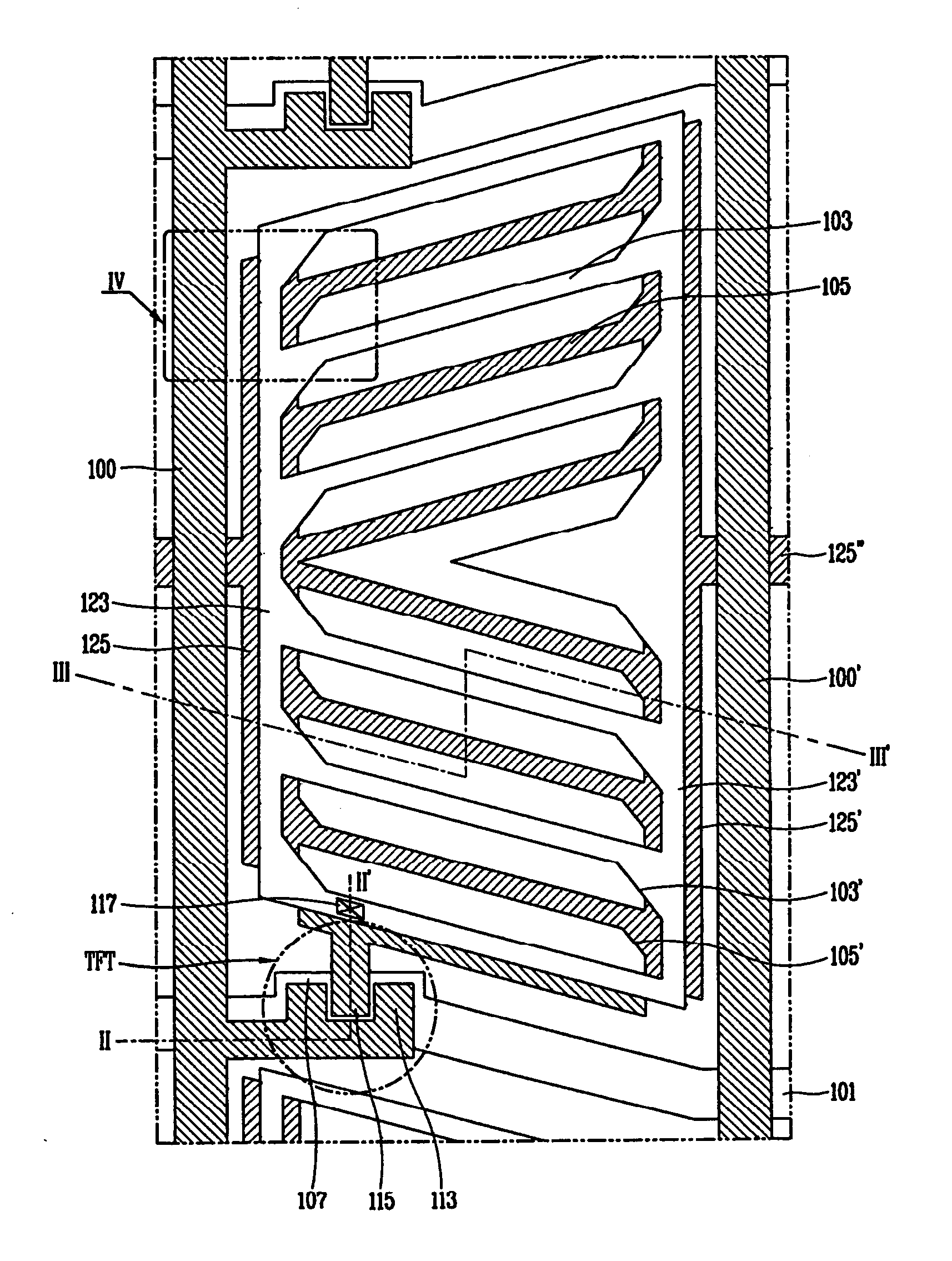
[0039]FIG. 3 shows an exemplary pixel region of an LCD device in accordance with the present invention. FIG. 4A is a cross-sectional view taken along line II-II′ of FIG. 3. FIG. 4B is a cross-sectional view taken along line III-III′ of FIG. 3. Referring to FIGS. 3, 4A and 4B, a liquid crystal panel includes a data line 100 and a gate line 101 arranged on a first substrate 110 and defining a pixel region, a switching device, such as a thin film transistor TFT, disposed at the crossing of the gate line 101 and the data line 100, and at least one pixel electrode 103 and one common electrode 105 alternately arranged in parallel to each other in the pixel region to generate a horizontal electric field. An alignment film (not shown) is formed on the first substrate 110 including the pixel electrode 103 and the common electrode 105. The alignment film is rubbed in the direction perpendicular to the data line 100. The pixel electrode 103 and the common electrode 105 are formed to have a til...

second embodiment

[0049] However, a vertical dim phenomenon may occur in the LCD device due to a parasitic capacitance between the data line 100 and the pixel electrode 103. the present invention is directed to an IPS mode LCD capable of enhancing picture quality of the liquid crystal panel, especially by removing the vertical line phenomenon.

[0050]FIG. 5 shows an exemplary pixel region of an LCD device in accordance with a second embodiment of the present invention. The structure of the second embodiment of the present invention is similar to that of the first embodiment, so only different portions of the second embodiment will be described in further details. The same reference numerals in FIG. 5 refer to the same or like elements of the LCD device of FIG. 3. In the second embodiment of the present invention, the second pixel electrode line 123′ (shown in FIG. 3) has been removed.

[0051] Referring to FIG. 5, a liquid crystal panel includes a data line 200 and a gate line 201 arranged on a first sub...


PUM


Abstract

A liquid crystal display device including a gate line formed on a first substrate; first and second adjacent data lines crossing the gate line to form adjacent pixel regions in an extended direction of the gate line; only one pixel electrode line in parallel with the first data line in each of the pixel regions; a plurality of pixel electrodes formed to be protruded in the extended direction of the gate line from the pixel electrode line; a plurality of common electrodes alternately formed in parallel with the plurality of pixel electrodes and generating an in-plane electric field therebetween; and an alignment film having a rubbing direction perpendicular to the first data line.

Description

[0001] This application claims the benefit of Korean Patent Application No. 2004-117401 filed in Korea on Dec. 30, 2004, which is hereby incorporated by reference in its entirety. BACKGROUND OF THE INVENTION [0002] 1. Field of the Invention [0003] The present invention relates to a liquid crystal display device and, more particularly, to an in-plane switching mode liquid crystal display device. [0004] 2. Description of the Background Art [0005] Recently, demand for light, thin, short, and small flat panel display devices has been increasing for use in various mobile electronic devices, such as mobile phones, PDAs, or notebook computers. Thus, research is active in areas related to flat panel display devices, such as Liquid Crystal Display (LCD) devices, Plasma Display Panel (PDP) devices, Field Emission Display (FED) devices, Vacuum Fluorescent Display (VFD) devices. Among these flat panel display devices, the LCD has taken the spotlight because it can be readily mass-produced, requ...

Claims


Application Information

Patent Timeline
IPC IPC(8): G02F1/1343
CPCG02F1/134363G02F1/1343
Inventor KANG, BYUNG KOOCHOI, WOON SUB
Owner LG DISPLAY CO LTD
Why Eureka
Try Eureka