Electronic circuit connecting structure of flat display panel substrate

Inactive Publication Date: 2009-03-26
AU OPTRONICS (SUZHOU) CORP LTD +1
View PDF16 Cites 2 Cited by
  • Summary
  • Abstract
  • Description
  • Claims
  • Application Information

AI Technical Summary

Benefits of technology

[0010]Hence, the connecting structure and the connecting method of the flat display panel substrate can effectively electrically connect the flat display panel substrate to the driving circuit module through the conductive protrusions. Since t

Problems solved by technology

Therefore, some of the ACF connections are poor in the electrical performance so as to easily produce the defect products and increase the manufacture cost of the liquid cry

Method used


Image

  • Electronic circuit connecting structure of flat display panel substrate
  • Electronic circuit connecting structure of flat display panel substrate

Examples


Example

[0014]The following description is of the best presently contemplated mode of carrying out the present invention. This description is not to be taken in a limiting sense but is made merely for the purpose of describing the general principles of the invention. The scope of the invention should be determined by referencing the appended claims.

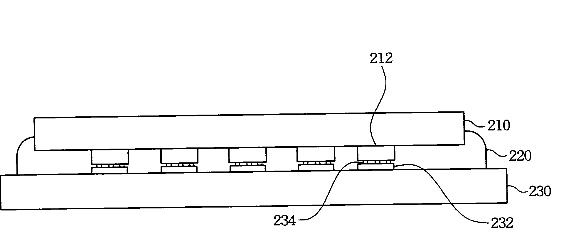
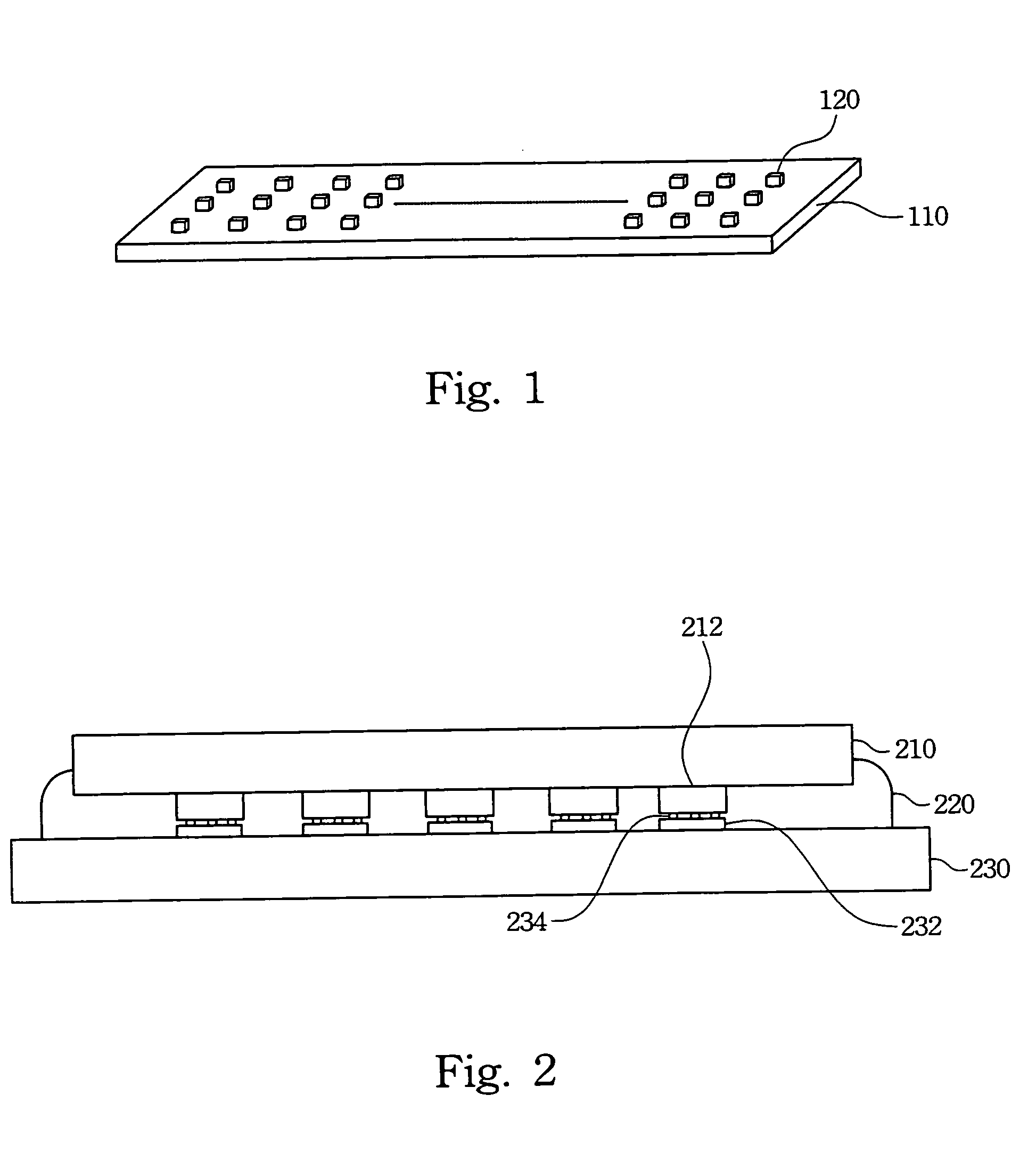
[0015]FIG. 1 illustrates a preferred embodiment of a conductive terminal with a plurality of conductive protrusions. The conductive protrusions 120 are formed on the conductive terminal 110. Simultaneously refer to FIG. 2. FIG. 2 schematically illustrates a connecting structure of a driving circuit board and a substrate having a conductive terminal with conductive protrusions thereon. The conductive protrusions 234 are preferably formed on a first terminal 232 of the substrate 230. A second terminal 212 of a driving circuit module 210 is first aligned to the first terminal 232 of the substrate 230 and then adhered to the first terminal 232 of the...


PUM

PropertyMeasurementUnit
Lengthaaaaaaaaaa
Temperatureaaaaaaaaaa
Pressureaaaaaaaaaa

Abstract

An electronic circuit connecting structure of a flat display panel substrate is described. The electronic circuit connecting structure includes a plurality of conductive terminals on the flat display panel substrate and a plurality of conductive protrusions formed on the conductive terminals. In addition, an electronic circuit connecting method for the flat display panel substrate is also disclosed therein.

Description

RELATED APPLICATIONS[0001]This application claims priority to China Patent Application Serial Number 200710153480.5, filed Sep. 20, 2007, which is herein incorporated by reference in its entirety.FIELD OF THE INVENTION[0002]The present invention generally relates to an electronic circuit connecting structure and method. More particularly, this invention relates to an electronic circuit connecting structure and method for a flat display panel substrate.BACKGROUND OF THE INVENTION[0003]Electronic products are gradually becoming smaller and lighter. The electronics packaging technology is therefore rapidly developing to satisfy various manufacturing requirements of the newer and smaller electronic products. The packaging technologies for manufacturing the liquid crystal display (LCD) at least include, for example, tape automated bonding (TAB), chip on glass (COG) or chip on film (COF).[0004]In the process to bond the chip to the glass substrate, the flip chip packaging process is adopt...

Claims


Application Information

Patent Timeline
IPC IPC(8): H05K1/09H01R12/04H01R9/00
CPCH05K3/305H05K3/325H05K3/361Y10T29/49147H05K2201/0373H01R12/7076H05K2201/0326
Inventor CHEN, JINLI, HUIHE, RONG
Owner AU OPTRONICS (SUZHOU) CORP LTD
Why Eureka
Try Eureka