Integrated circuit chip

a technology of integrated circuits and chips, applied in the direction of electrical equipment, semiconductor devices, semiconductor/solid-state device details, etc., can solve the problems of noise coupling, damage to the circuits of integrated circuit chips, further affecting the normal operation of rf circuits, etc., to reduce noise coupling, improve the electrical characteristics of the integrated circuit chip, and prevent the build-up of electric charges

Active Publication Date: 2006-09-07
AIROHA TECHNOLOGY CORPORATION
View PDF4 Cites 20 Cited by
  • Summary
  • Abstract
  • Description
  • Claims
  • Application Information

AI Technical Summary

Benefits of technology

[0014] It is therefore an object of the invention to provide an integrated circuit chip. The design of mutual electrical connection between the seal ring, the ground ring and the guard ring not only reduces the noise coupling between the circuits and the I / O pad and the external thereof, but also prevents the build-up of electric charges generated during the plasma etching manufacturing process, hence improving the electrical characteristics of the integrated circuit chip.

Problems solved by technology

When scribing the integrated circuit chip, the generated stress will cause damage to the circuits of the integrated circuit chip.
Moreover, the RF circuit 13 is a circuit which is easily interrupted by the noise, so that the noise generated by the digital circuit 12 or the I / O pad 12a will be easily transmitted to the RF circuit 13 or the I / O pad 13a through the seal ring 11, resulting in noise coupling and further affecting the normal operation of the RF circuit 13.

Method used


Image

  • Integrated circuit chip
  • Integrated circuit chip
  • Integrated circuit chip

Examples


Embodiment Construction

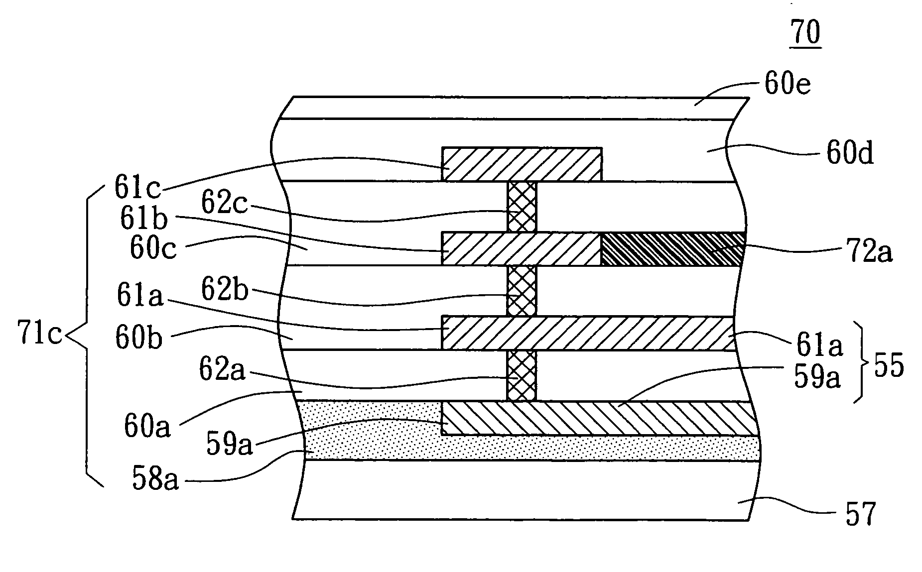
[0032] Refer to FIGS. 4˜6 at the same time. FIG. 4 is a top view of an integrated circuit chip according to a preferred embodiment of the invention. FIG. 5 is a partial enlargement of a cross-sectional view of the integrated circuit chip along the cross-sectional line 5-5′ in FIG. 4. FIG. 6 is a partial enlargement of a cross-sectional view of the integrated circuit chip along the cross-sectional line 6-6′ in FIG. 4. In FIGS. 4˜6, an integrated circuit chip 70 includes a silicon substrate 57, a seal ring 71, a ground ring 72, at least a circuit, an input / output (I / O) pad of the circuit, and at least a guard ring, such as a digital circuit 73, a radio frequency (RF) circuit 74 and two guard rings 55 and 56 for instance. The digital circuit 73 and the RF circuit 74 respectively has an I / O pad 73a and 74a. The seal ring 71, the ground ring 72, the digital circuit 73, the RF circuit 74, the I / O pads 73a˜74a and the guard rings 55˜56 are all formed on the silicon substrate 57. The seal r...


PUM


Abstract

An integrated circuit chip is provided. The chip includes a silicon substrate, a circuit, a seal ring, a ground ring and a guard ring. The circuit is formed on the silicon substrate and has an input / output (I / O) pad. The seal ring is formed on the silicon substrate and surrounds the circuit and the I / O pad. The ground ring is formed between the silicon substrate and the I / O pad, and the ground ring is electrically connected with the seal ring. The guard ring is formed above the silicon substrate and surrounds the I / O pad, and the guard ring is electrically connected with the seal ring.

Description

[0001] This application claims the benefit of Taiwan application Serial No. 92133104, filed Nov. 25, 2003, the subject matter of which is incorporated herein by reference. BACKGROUND OF THE INVENTION [0002] 1. Field of the Invention [0003] The invention is related to an integrated circuit (IC) chip, and more particularly to an integrated circuit chip having a seal ring, a ground ring and a guard ring. [0004] 2. Description of the Related Art [0005] A semiconductor wafer comprises a number of integrated circuit chips formed through integrated circuit manufacturing process with each integrated circuit chip comprises a number of circuits, such as digital circuits, analog circuits and radio frequency (RF) circuits. A scribing line is formed between any two adjacent integrated circuit chips to facilitate the scribing of integrated circuit chips. When scribing the integrated circuit chip, the generated stress will cause damage to the circuits of the integrated circuit chip. Therefore, a s...

Claims


Application Information

Patent Timeline
Patent Type & Authority Applications(United States)
IPC IPC(8): H01L23/48H01L23/58
CPCH01L23/585H01L2924/0002H01L2924/00
Inventor CHEN, SHENG-YOW
Owner AIROHA TECHNOLOGY CORPORATION
Why Eureka
Try Eureka