
Liquid crystal display

Inactive Publication Date: 2006-09-21
SAMSUNG ELECTRONICS CO LTD
View PDF7 Cites 7 Cited by
  • Summary
  • Abstract
  • Description
  • Claims
  • Application Information

AI Technical Summary

Benefits of technology

[0010] In exemplary embodiments of the present invention, a liquid crystal display rapidly changes alignment of liquid crystal molecules and minimi

Problems solved by technology

In addition, the liquid crystal display with a vertical alignment mode

Method used


Image

  • Liquid crystal display
  • Liquid crystal display
  • Liquid crystal display

Examples


Example

[0031] Hereinafter, exemplary embodiments of the present invention will be described in detail with reference to the attached drawings such that the present invention can be easily put into practice by those skilled in the art. However, the present invention is not limited to the exemplary embodiments, but may be embodied in various forms.

[0032] In the drawings, thicknesses are enlarged for the purpose of clearly illustrating layers and areas. If it is mentioned that a layer, a film, an area, or a plate is placed on a different element, it includes a case that the layer, film, area, or plate is placed right on the different element, as well as a case that another element is disposed therebetween. On the contrary, if it is mentioned that one element is placed right on another element, it means that no element is disposed therebetween.

[0033] It will be understood that, although the terms first, second, third etc. may be used herein to describe various elements, components, regions, ...


PUM


Abstract

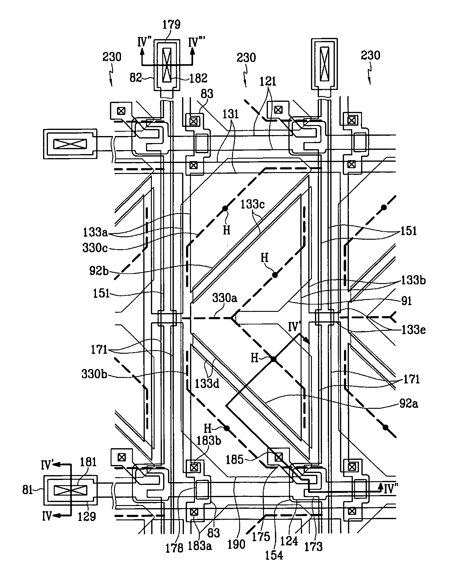
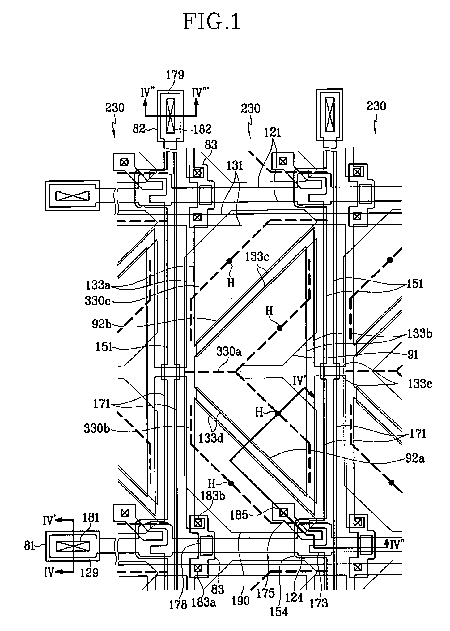
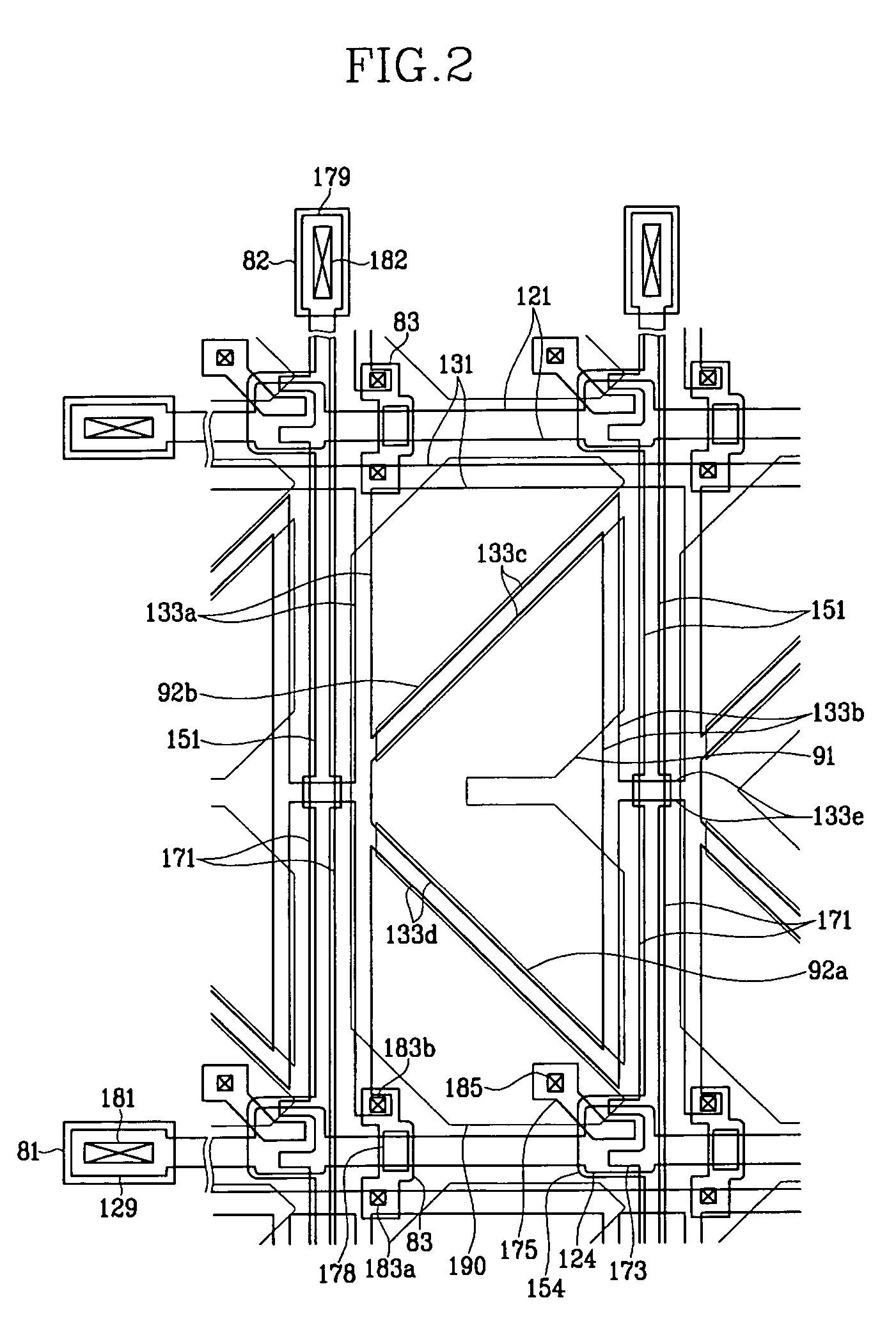
A liquid crystal display includes: a panel; an electric field generating electrode formed on the panel; and a sloped member formed on the panel. The sloped member has a ridge and a slope, wherein at least one singular portion is formed in the ridge.

Description

[0001] This application claims priority to Korean Patent Application No. 2005-0022746, filed on Mar. 18, 2005, and all the benefits accruing therefrom under 35 U.S.C. §119, and the contents of which in its entirety are herein incorporated by reference. BACKGROUND OF THE INVENTION [0002] (a) Field of the Invention [0003] The present invention relates to a display panel and a liquid crystal display having the display panel. [0004] (b) Description of the Related Art [0005] A liquid crystal display, which is widely used in flat panel displays, includes two panels (e.g., upper and lower panels) having electric field generating electrodes such as pixel electrodes and a common electrode on respective panels, and a liquid crystal layer interposed therebetween. The liquid crystal display displays an image by applying a voltage to the electric field generating electrodes, which generates an electric field in the liquid crystal layer determining alignment of liquid crystal molecules in the liq...

Claims


Application Information

Patent Timeline
IPC IPC(8): G02F1/1343
CPCG02F1/133371G02F1/133707G02F1/134336G02F1/1393F16H3/089
Inventor SOHN, JI-WONCHOI, NAK-CHOLYU, JAE-JIN
Owner SAMSUNG ELECTRONICS CO LTD
Learn More