Optical waveguide device and method of adjusting a transmission loss thereof

a technology of optical waveguide and transmission loss, which is applied in the direction of optical waveguide light guide, instruments, optics, etc., can solve the problems of large volume of the entire module, difficult to obtain a desirable excessive loss amount, and high cost, and achieve desirable tolerance, high precision, and desirable dynamic range

Active Publication Date: 2007-05-10
NEC CORP
View PDF6 Cites 9 Cited by
  • Summary
  • Abstract
  • Description
  • Claims
  • Application Information

AI Technical Summary

Benefits of technology

[0013] The optical waveguide device and the method of adjusting the transmission loss thereof according to the present invention allow the excessive losses to be applied to the respective signal beams which are propagated through the plurality of optical waveguides with the above-mentioned structure and by the above-mentioned method. Therefore, the present invention has such an effect that both a desirable dynamic range and a desirable tolerance can be achieved in the excessive loss amount. As a consequence, according to the present invention, there is such an effect that the difference in the transmission losses of the signal beams propagated through the plurality of optical waveguides can be controlled with higher precision.

Problems solved by technology

This has been a cause of making the entire module bulky, requiring high cost.
That is, it is difficult to obtain a desirable excessive loss amount by merely adjusting the cross angle “a2.” This is because there are possibilities that a tolerance for adjusting the excessive loss amount becomes excessively severe, and such a dynamic range having a sufficient excessive loss amount cannot be achieved.
As a result, the difference in the transmission losses among the output waveguides cannot be sufficiently reduced.
As previously explained, the previous proposals have such a problem that it is difficult to control the difference in the transmission losses among the plurality of optical waveguides in high precision.

Method used


Image

  • Optical waveguide device and method of adjusting a transmission loss thereof
  • Optical waveguide device and method of adjusting a transmission loss thereof
  • Optical waveguide device and method of adjusting a transmission loss thereof

Examples


first embodiment

[0033] Now, a detailed description is made of an optical waveguide device and a method for adjusting a transmission loss of the optical waveguide device according to the present invention.

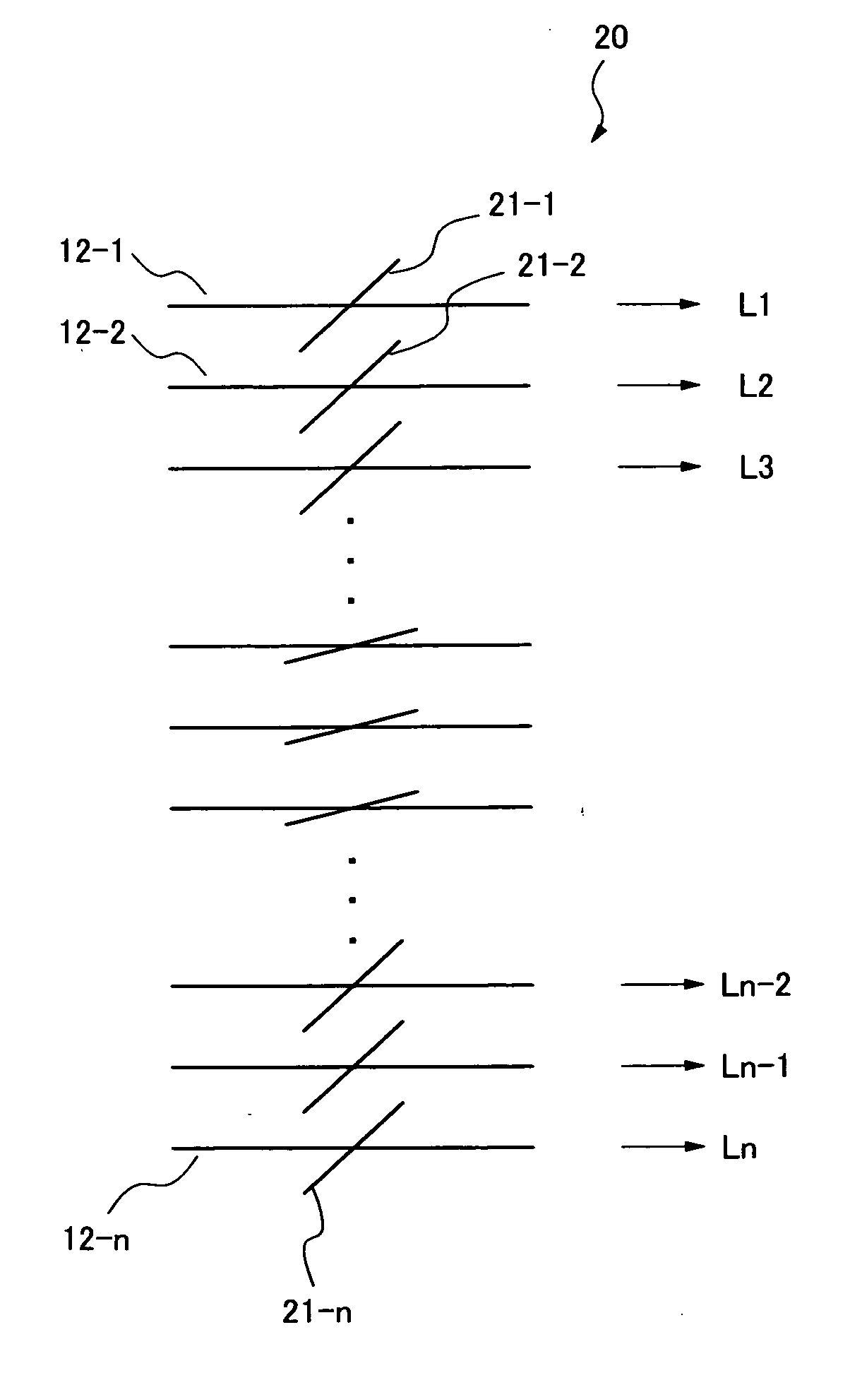
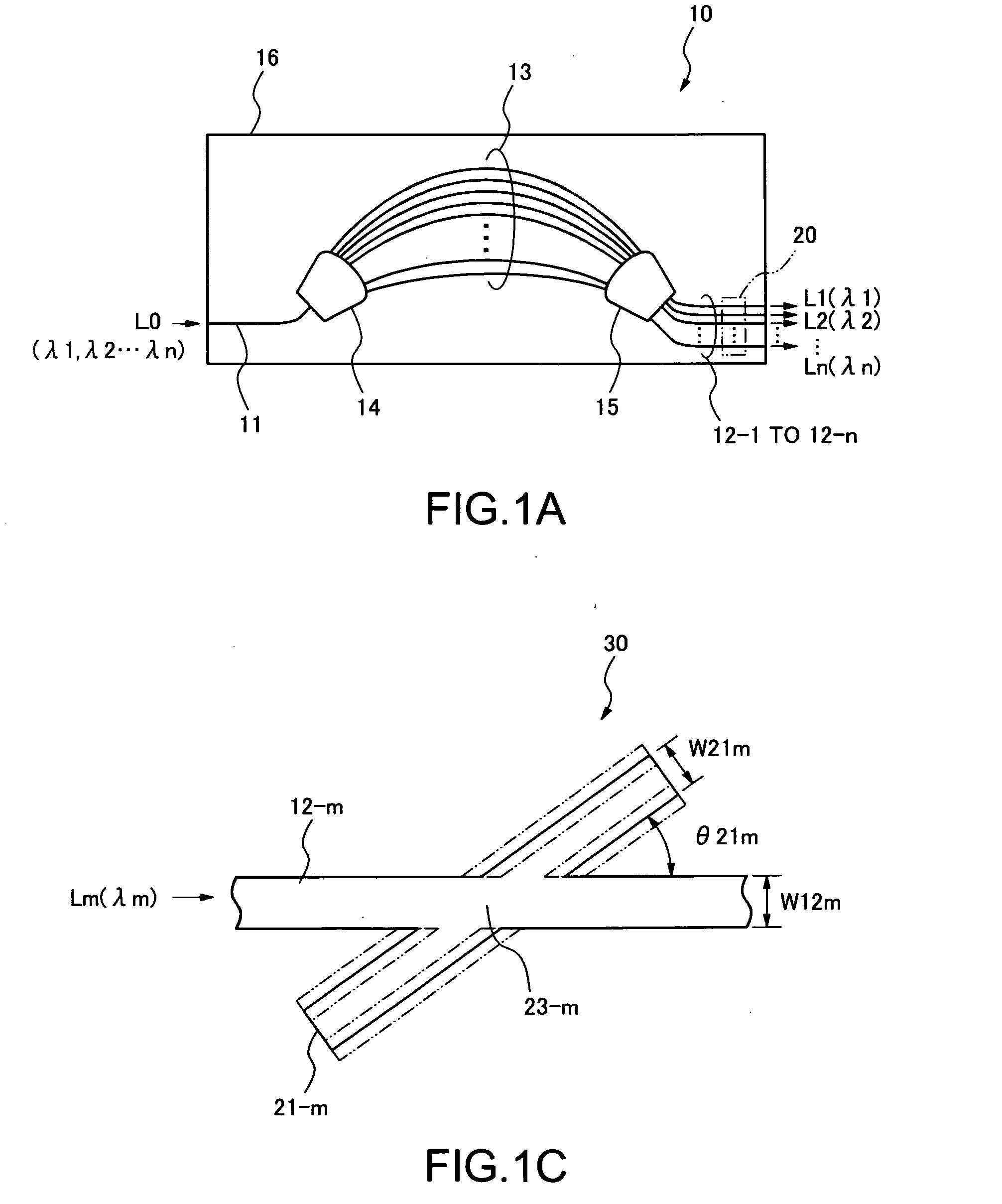
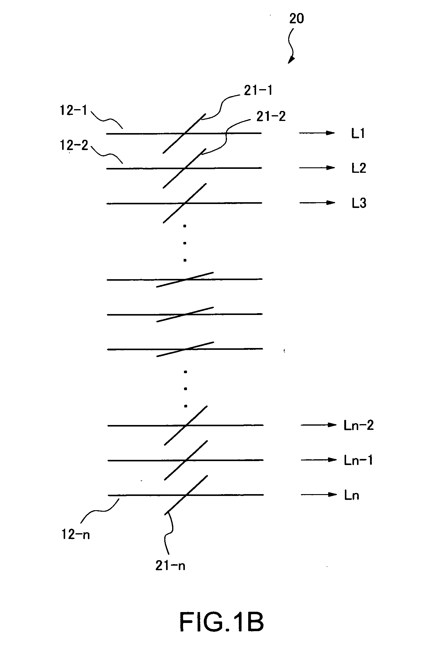
[0034]FIG. 1A is a plan view for indicating an arrayed waveguide grating (AWG) 10 equipped with an optical waveguide circuit according to the first embodiment of the present invention. FIG. 1B is a plan view for representing the optical waveguide circuit in FIG. 1A. FIG. 1C is a partially enlarged view for showing an optical waveguide of the optical waveguide circuit in FIG. 1B. Based upon these drawings, the first embodiment will now be explained.

[0035] As represented in FIG. 1A, an AWG 10 includes one input waveguide 11, “n” (symbol “n” is an integer equal to or larger than 2) output waveguides 12-1 to 12-n, a plurality of arrayed waveguides 13, a slab waveguide 14, another slab waveguide 15, and an optical waveguide circuit 20 on a substrate 16. The slab waveguide 14 connects the input waveguid...

second embodiment

[0053] In a cross waveguide 41-m as indicated in FIG. 3A, terminal structures 42-m and 43-m are provided on edge surfaces thereof for avoiding that signal beams are reflected to be returned. The terminal structures 42-m and 43-m have edge surfaces which are inclined with respect to such a plane perpendicular to an optical axis of the cross waveguide 41-m. As a result, a partial beam of the signal beam Lm which is inputted from the output waveguide 12-m to the cross waveguide 41-m is reflected by the edge surfaces of the terminal structures 42-m and 43-m along the oblique direction with respect to the optical axis. Therefore, this reflected beam cannot be propagated within the cross waveguide 41-m, but is radiated to the clad. As a consequence, it is possible to avoid that the signal beam is reflected on the edge surface of the cross waveguide 41-m, and then the reflected beam is transmitted through the cross waveguide 41-m along the opposite direction. Also, it is possible to avoid...

fourth embodiment

[0055] In the optical waveguide 60 as indicated in FIG. 3D, a cross angle is changed depending upon a direction which crosses with respect to the output waveguide 12-m. Concretely speaking, a cross waveguide 61-m is divided into a front-sided cross waveguide 62-m and a rear-sided cross waveguide 63-m, while a portion thereof which crosses with the output waveguide 12-m is set to a center. Then, a cross angle between the front-sided cross waveguide 62-m and the output waveguide 12-m is assumed as “θ62m”, while the front-sided cross waveguide 62-m is extended to a direction along which the signal beam Lm is traveled. Also, across angle between the rear-sided cross waveguide 63-m and the output waveguide 12-m is assumed as “θ63m”, while the rear-sided cross waveguide 63-m is extended to a direction which is opposite to the direction along which the signal beam Lm is traveled. The cross angle θ62m of the front-sided cross waveguide 62-m is set to be larger than the cross angle θ63m of ...


PUM


Abstract

An optical waveguide device includes a plurality of optical waveguides propagating therethrough a signal beam, and a plurality of optical sub-waveguides connected to the plurality of optical waveguides respectively, applying an excessive loss to the signal beam by branching a partial beam of the signal beam. A dynamic range and a tolerance in an amount of the excessive loss is adjusted by adjusting widths of the plurality of optical sub-waveguides with respect to the plurality of optical waveguides, and the amount of the excessive loss applied to the signal beam are adjusted by adjusting an angle connecting each of the plurality of optical sub-waveguides with respect to each of the plurality of optical waveguides.

Description

BACKGROUND OF THE INVENTION [0001] 1. Field of the Invention [0002] The present invention relates to an optical waveguide device used in optical communications and the like, and to a method of adjusting a transmission loss of the optical waveguide device. To be more specific, the present invention relates to the optical waveguide device equipped with a plurality of optical waveguides such as arrayed waveguide gratings, optical splitters, and optical star couplers, and also relates to the method of adjusting the transmission loss of the optical waveguide device. [0003] 2. Description of the Related Art [0004] In wavelength division multiplexing (WDM) transmission systems, arrayed waveguide gratings are generally used as either optical demultiplexers or optical multiplexers. It should be noted that an arrayed waveguide grating will be abbreviated as an “AWG” hereinafter. A basic structure of an AWG is described in, for example, a related art document 1, namely, Japanese Patent Applica...

Claims


Application Information

Patent Timeline
Patent Type & Authority Applications(United States)
IPC IPC(8): G02B6/26
CPCG02B6/12009G02B6/125G02B6/266G02B6/10
Inventor WATANABE, SHINYA
Owner NEC CORP
Why Eureka
Try Eureka