Semiconductor device and operating method thereof

Inactive Publication Date: 2007-05-31
SEMICON ENERGY LAB CO LTD
View PDF6 Cites 288 Cited by
  • Summary
  • Abstract
  • Description
  • Claims
  • Application Information

AI Technical Summary

Benefits of technology

[0010] A radio chip is manufactured by using an expensive silicon wafer similarly to a microprocessor and a semiconductor memory. Accordingly, it has been naturally limiting to reduce the unit cost of a chip. Especially, a large a

Problems solved by technology

Accordingly, it has been naturally limiting to reduce the unit cost of a chip.
Therefore, in the case where a conventional radio chip is used as an IC tag, it is not appropriate to be attached to a substrate of a commercial product having a curved surface shape.
A method of thinning a chip by grinding and polishing a silicon wafer itself may be applied; however, the number of steps is increase

Method used


Image

  • Semiconductor device and operating method thereof
  • Semiconductor device and operating method thereof
  • Semiconductor device and operating method thereof

Examples


embodiment mode 1

[0050] In this embodiment mode, a structure of a radio chip is described.

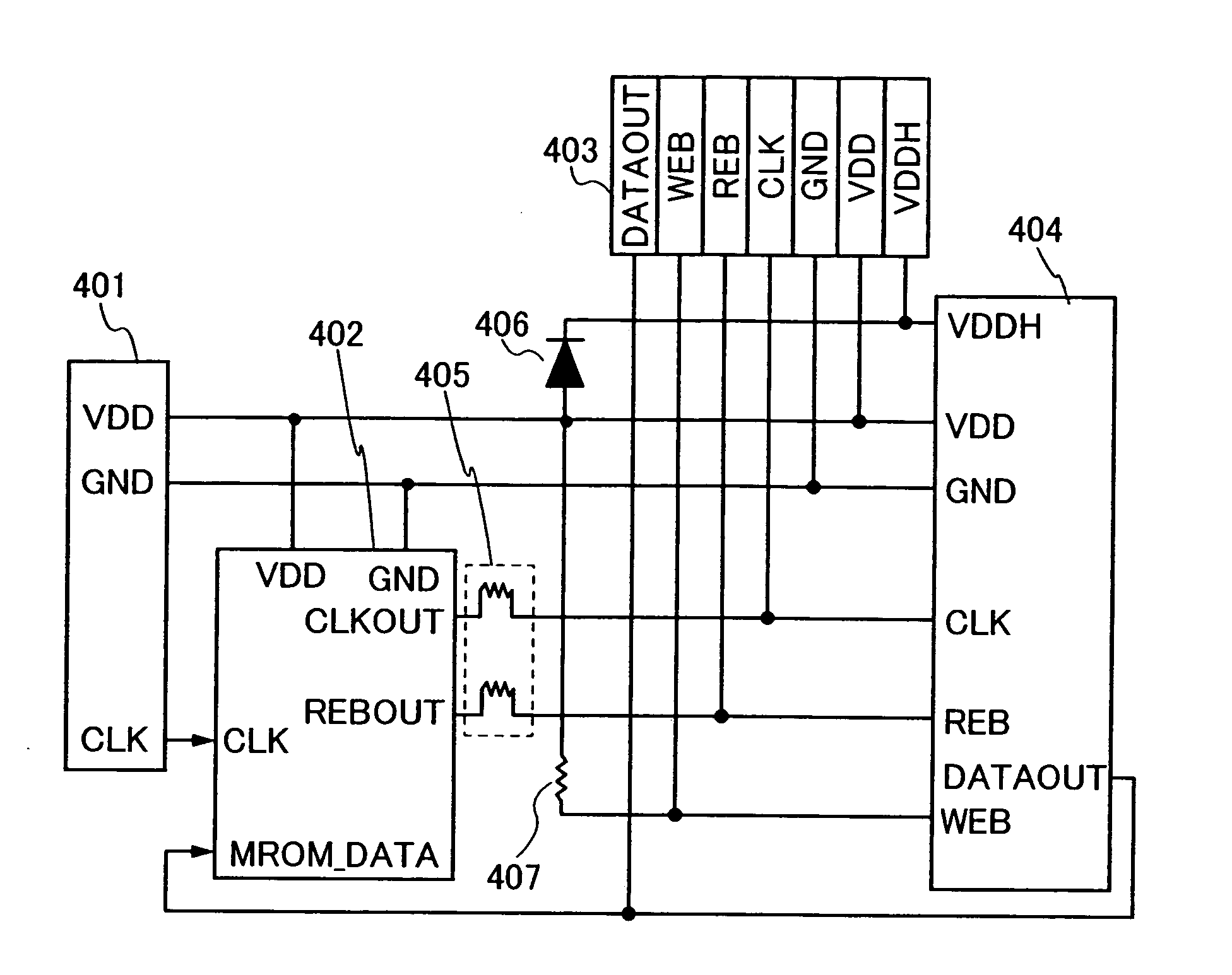
[0051] As shown in FIG. 1A, a radio chip includes an RF input portion 401, a logic circuit portion 402, an external signal input portion 403, a memory region 404 including an organic memory, and an adjustment circuit portion 405.

[0052] Two kinds of power supply potentials which are a high potential side power supply potential (VDD) and a low potential side power supply are applied from the RF input portion. The RF input portion 401 includes a high potential side power supply potential (VDD) terminal and a low potential side power supply potential terminal. Further, the RF input portion 401 includes a clock signal (CLK) terminal. In this embodiment mode, a ground potential (GND) is used as a low potential side power supply potential.

[0053] The RF input portion 401 rectifies a radio wave received from an antenna (not shown) in order to generate VDD and frequency-divides a received radio wave in order to genera...

embodiment mode 2

[0068] In this embodiment mode, description is made of an operation of the organic memory shown in Embodiment Mode 1.

[0069]FIG. 3A is a timing chart in the case of writing and shows waveforms of REB, WEB and CLK. At this time, a period of CLK is set to be about 1 ms. A reset period is when REB and WEB are in a HIGH state. Subsequently, when WEB becomes a LOW state, HIGH(1) is written to the organic memory. Next, when REB becomes a LOW state and WEB becomes a HIGH state at the same time, writing is not performed to the organic memory. Writing to the organic memory is performed by repeating these periods successively.

[0070]FIG. 3B is a timing chart in the case of reading and shows waveforms of REB, WEB and CLK. At this time, a period of CLK is set to be about 10 μs. A reset period is when REB and WEB are in a HIGH state. Subsequently, REB becomes a LOW state, that is, a reading period starts.

[0071] As described above, when both REB and WEB are in a HIGH state, an operation of a cir...

embodiment mode 3

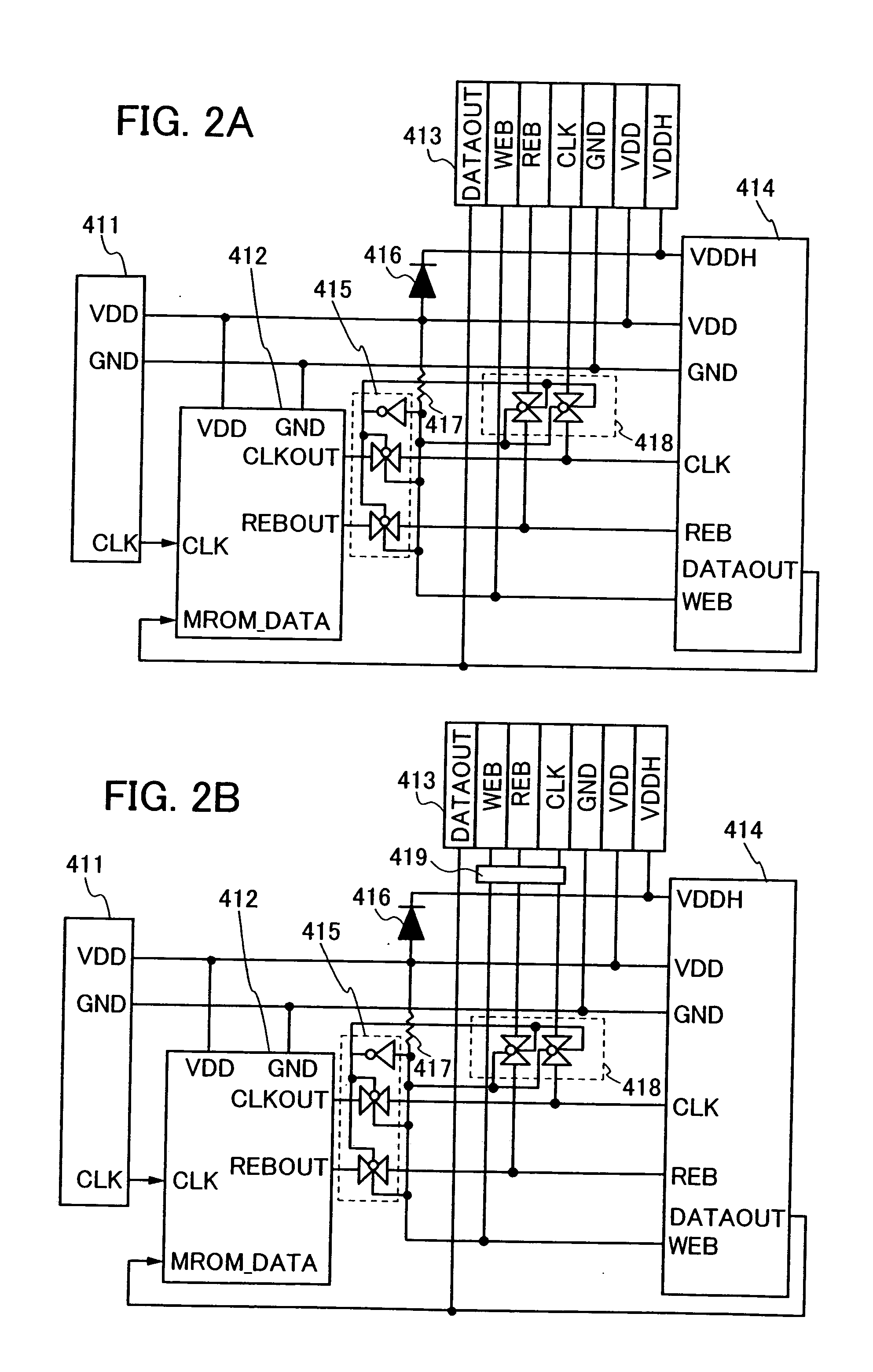
[0099] In this embodiment mode, description is made of a structure of a radio chip which is different from that in Embodiment Mode 1.

[0100]FIG. 2A shows a structure of a radio chip which has a different structure of the adjustment circuit portion from that shown in FIG. 1A. The radio chip shown in FIG. 2A includes an RF input portion 411, a logic circuit portion 412, an external signal input portion 413, a memory region 414 including an organic memory, an adjustment circuit portion 415, a diode 416, a resistor 417, and a switching element 418. The adjustment circuit portion 415 of the radio chip of this embodiment mode is constituted by a switch. As a switch an analog switch, or the like can be used. In this embodiment mode, an inverter and an analog switch are used. Analog switches are provided between the logic circuit portion 412 and CLK terminal of the memory region 414, and between the logic circuit portion 412 and REB terminal of the memory region 414. An input terminal of th...


PUM


Abstract

In an organic memory which is included in a radio chip formed from a thin film, data are written to the organic memory by a signal inputted with a wired connection, and the data is read with a signal by radio transmission. A bit line and a word line which form the organic memory are each selected by a signal which specifies an address generated based on the signal inputted with a wired connection. A voltage is applied to a selected memory element. Thus writing is performed. Reading is performed by a clock signal or the like which are generated from a radio signal.

Description

BACKGROUND OF THE INVENTION [0001] 1. Field of the Invention [0002] The present invention relates to a semiconductor device which includes a memory region having an organic compound layer, and an operating method thereof. [0003] 2. Description of the Related Art [0004] A semiconductor device including a radio communication function, specifically a radio chip is expected to have a large market. Such a radio chip is referred to as an ID tag, an IC tag, an IC chip, an RF (Radio Frequency) tag, a radio tag, an electronic tag, and an RFID (Radio Frequency Identification) in accordance with usage. [0005] A radio chip includes an interface, a memory, a control section, and the like. As a memory, a random access memory (hereinafter referred to as RAM), which can be written and read, and a read only memory (hereinafter referred to as ROM), which is read only, are employed and used properly in accordance with usage. Specifically, a memory region is assigned to each particular application, and...

Claims


Application Information

Patent Timeline
IPC IPC(8): H04B7/00
CPCB82Y10/00G06K19/07749G11C13/0014G11C13/004H01L27/12G11C2213/79H01L27/1214H01L51/0591G11C13/0069H01L27/1266H10K10/50G06K19/077G06K19/07
Inventor SAITO, TOSHIHIKOKATO, KIYOSHI
Owner SEMICON ENERGY LAB CO LTD
Why Eureka
Try Eureka