Method of manufacturing multi-layer wiring board
- Summary
- Abstract
- Description
- Claims
- Application Information
AI Technical Summary
Problems solved by technology
Method used
Image

Examples
Example
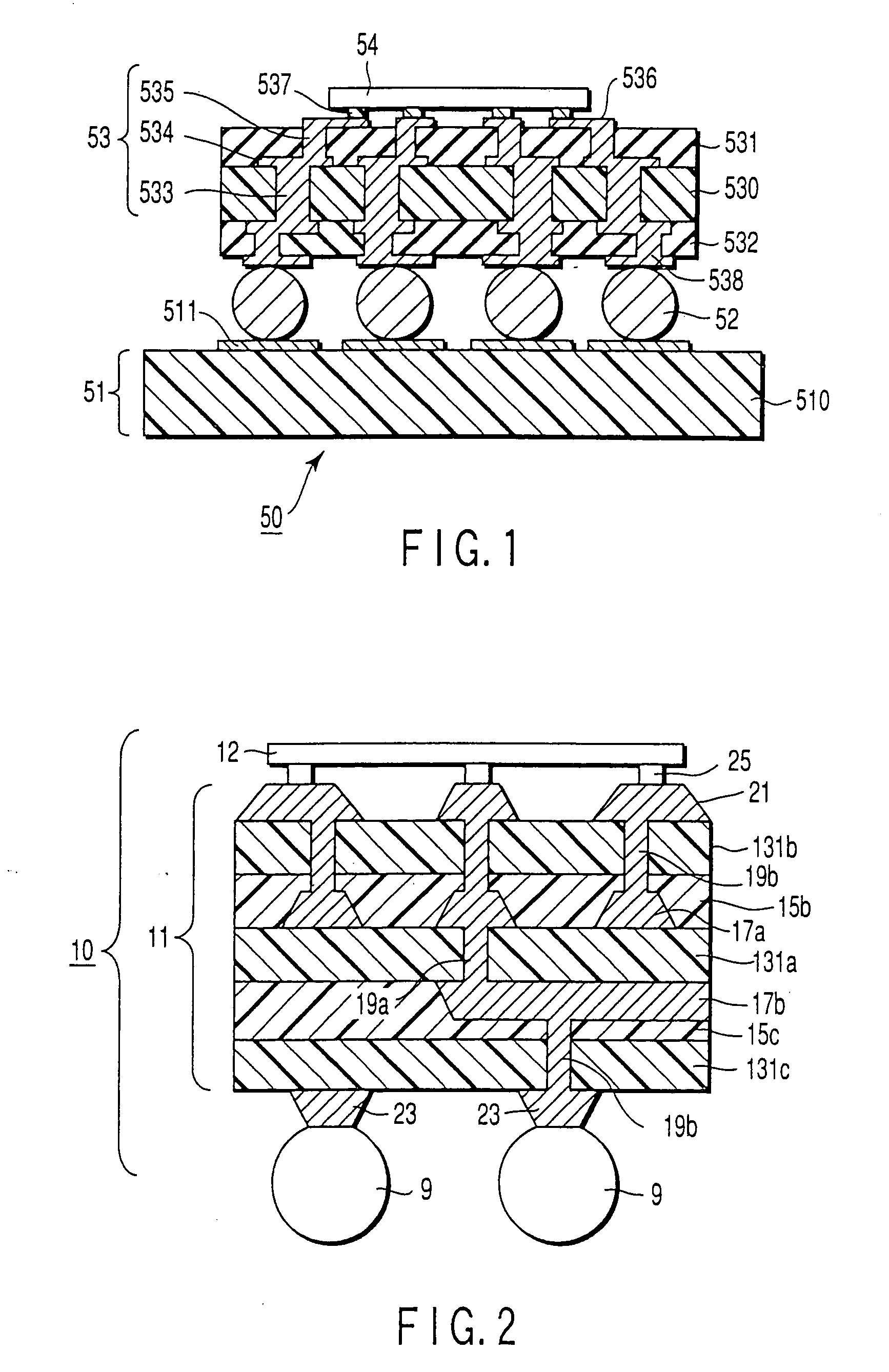
[0157] Example 1 will be explained with reference to FIGS. 8A through 8I. This example illustrates a manufacturing example of multi-layer circuit wiring board where the subtractive method is employed.
[0158] First of all, as shown in FIG. 8A, a film 13a or a double conductor-layered polyimide tape substrate comprising a polyimide layer 131a (25 μm for example) and provided, on the opposite surfaces of the polyimide layer 131a, with conductor layers (copper foil) 130a and 132a (12 μm for example) is prepared. Then, a via-hole 190 is formed in this film 13a as shown in FIG. 8B by means of ultraviolet laser.
[0159] This via-hole 190 is then subjected to a treatment to remove dross and to a desmear treatment, which is followed by DPS and electrolytic copper plating to thereby form a via-contact layer 19a functioning to electrically connect one surface of the film 13a with the other surface thereof as shown in FIG. 8C. Incidentally, the reasons to employ the film 13a comprising a polyimi...
Example
[0175] Example 2 will be explained with reference to FIGS. 8A through 8F, and FIGS. 9A through 9E. This example illustrates a manufacturing example of multi-layer circuit wiring board where the semi-additive method is employed.
[0176] First of all, as explained with reference to FIGS. 8A through 8F, a conductor layer (copper foil) (130b)-attached polyimide film 13b is laminated via the adhesive layer 15b on one surface of the polyimide layer 131a having the wiring patterns 17a and 17b on the opposite surfaces thereof, respectively, and at the same time, a conductor layer (copper foil) (130c)-attached polyimide film 13c is laminated via the adhesive layer 15c on the other surface of the polyimide layer 131a. Thereafter, via-contact layers 19a and 19b are formed so as to electrically connect the conductor layer 130b with the conductor layer 130c. Details of treatment in each of the steps are the same as explained with reference to Example 1.
[0177] Then, as shown in FIG. 9A, an aqueou...
Example
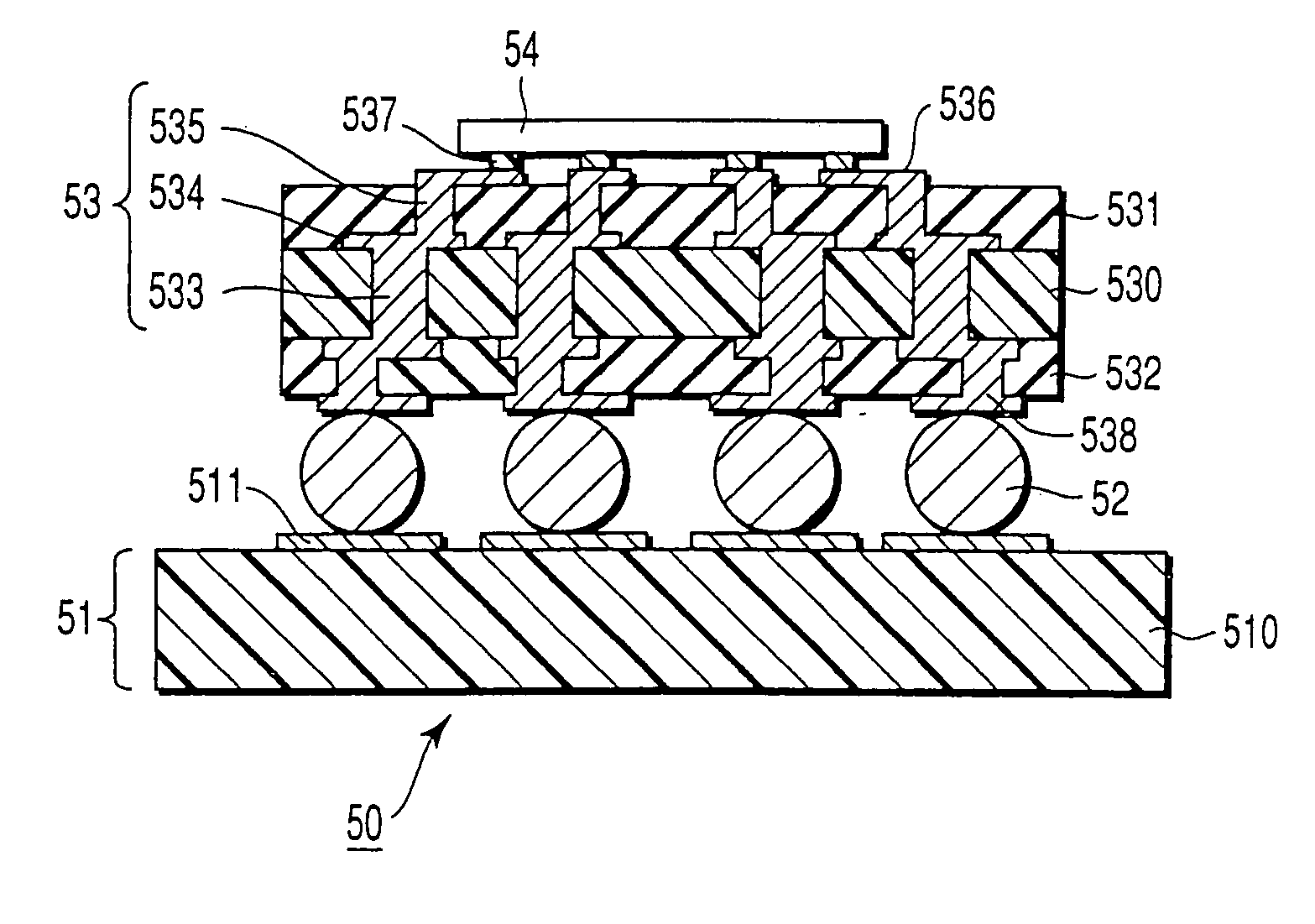
[0186] Example 3 will be explained with reference to FIGS. 13A through 13C. This example illustrates a manufacturing example of a multi-layer circuit wiring board 50 having a 6-ply circuit wiring wherein the subtractive method and the semi-additive method are combined.
[0187] First of all, by the same method as explained in Example 1, there is fabricated, as shown in FIG. 13A, a multi-layer circuit wiring board 11 formed of a 4-ply circuit substrate which is provided with a stripe-like wiring pattern consisting of a plurality of straight lines each having a line width of 15 μm and arrayed at a pitch of 30 μm.
[0188] Then, as shown in FIG. 13B, a film 13d comprising a conductor layer (copper foil) 130d and a polyimide film 131d is laminated via the adhesive layer 15d on one surface of the multi-layer circuit wiring board 11, and at the same time, a film 13e comprising a conductor layer (copper foil) 130e and a polyimide film 131e is laminated via the adhesive layer 15e on the other s...
PUM
| Property | Measurement | Unit |
|---|---|---|
| Length | aaaaa | aaaaa |
| Length | aaaaa | aaaaa |
| Length | aaaaa | aaaaa |
Abstract
Description
Claims
Application Information
 - R&D Engineer
- R&D Manager
- IP Professional
- Industry Leading Data Capabilities
- Powerful AI technology
- Patent DNA Extraction
Browse by: Latest US Patents, China's latest patents, Technical Efficacy Thesaurus, Application Domain, Technology Topic.
© 2024 PatSnap. All rights reserved.Legal|Privacy policy|Modern Slavery Act Transparency Statement|Sitemap