

Stacked package module
a technology of stacking and package modules, applied in the direction of printed circuit aspects, electrical apparatus construction details, printed circuit non-printed electric components association, etc., can solve the problems of reduced elasticity of circuit layout on the substrate, design flexibility of package structure, non-detachable electrical connections, etc., to achieve more elastic conductive pad layout, compact size and space-saving products
- Summary
- Abstract
- Description
- Claims
- Application Information
AI Technical Summary
Benefits of technology
Problems solved by technology
Method used
Image

Examples
embodiment 1
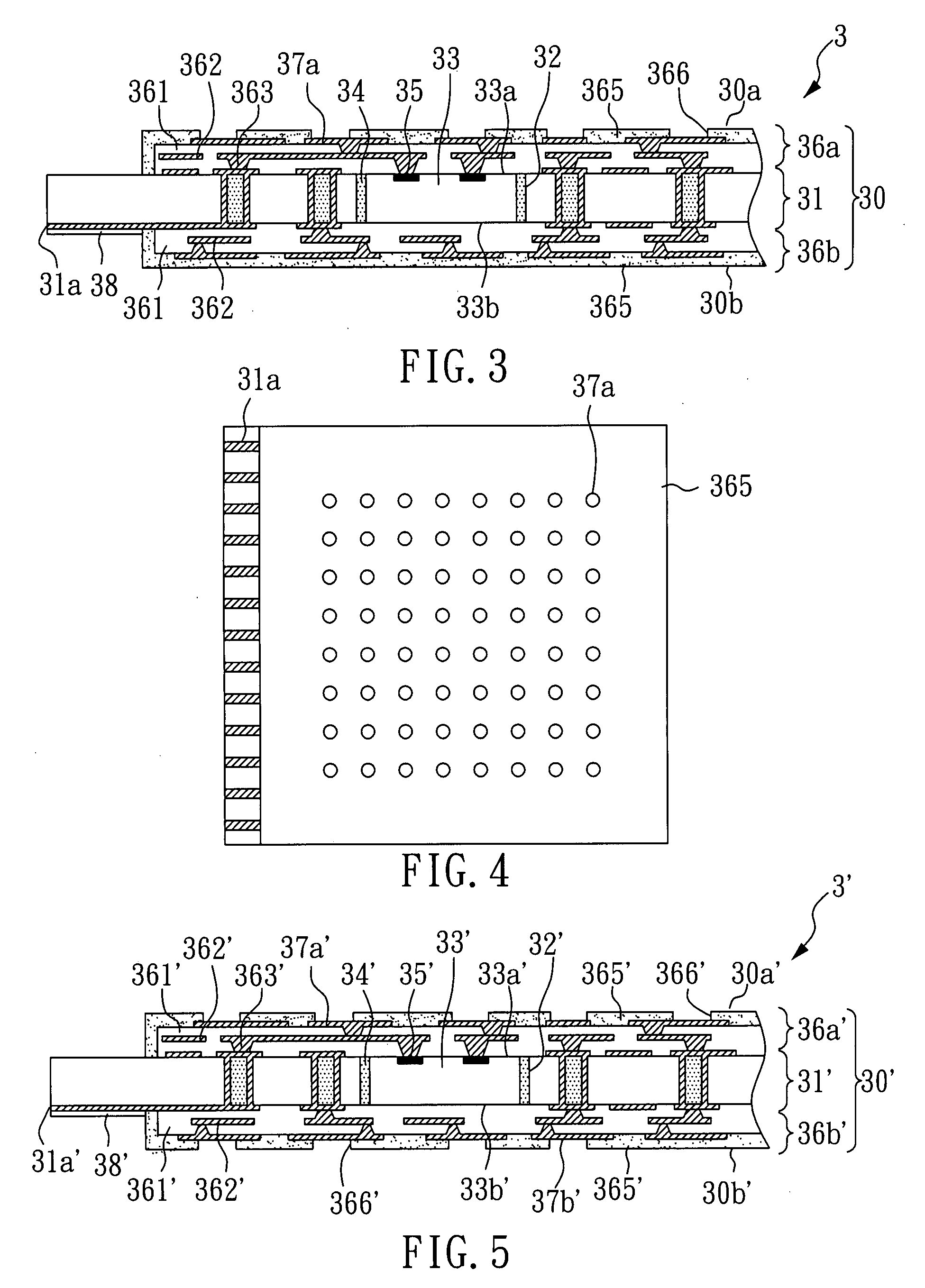
[0031]With reference to FIG. 3, there is shown a cross-section view of a package structure with a chip embedded therein. The package structure 3 with a chip embedded therein of the present embodiment comprises a first circuit board 30 with a first chip 33 embedded therein. The first circuit board 30 has a first surface 30a, an opposite second surface 30b, a plurality of exposed electro-connecting ends 31a, and a plurality of first conductive pads 37a on the first surface 30a. In detail, the first circuit board 30 has a core board 31 with a through cavity 32 therein, therewith the first chip 33 embedded in the cavity 32 of the core board 31, the gap between the core board 31 and the first chip 33 filled with a filling material 34 to fix the first chip 33, the first chip 33 having an active surface 33a and an opposite inactive surface 33b, wherein the active surface 33a has a plurality of electrode pads 35. The first circuit board 30 further comprises a first built-up structure 36a an...
embodiment 2
[0033]With reference to FIG. 5, there is shown a cross-section view of a package structure with a chip embedded therein. The package structure 3′ with a chip embedded therein of the present embodiment is the same as the package structure 3 of Embodiment 1, except that the package structure 3′ further comprises a plurality of second conductive pads 37b′, and the solder mask 365′ of the second built-up structure 36b′ has a plurality of openings 366′ to expose the second conductive pads 37b′.
embodiment 3
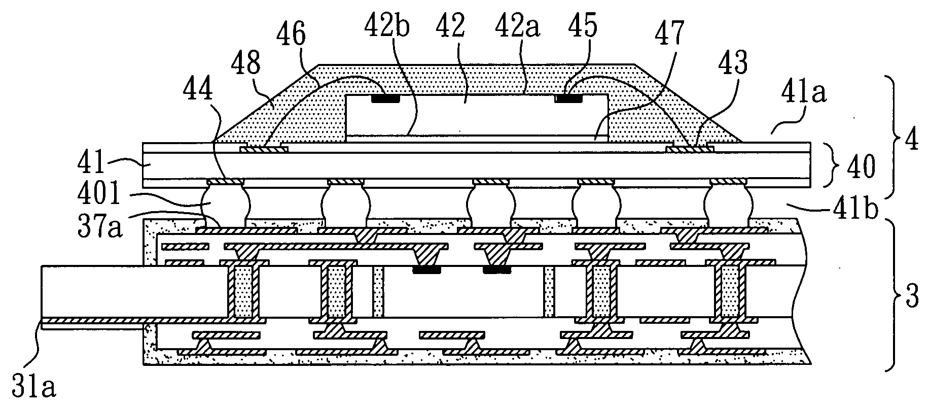
[0034]With reference to FIG. 6, there is shown a cross-section view of a stacked package module. The stacked package module of the present embodiment uses the package structure 3 of Embodiment 1 and a wire bonding package structure 4 as package units. The wire bonding package structure 4 comprises a second chip 42 and a second circuit board 40. In detail, the second circuit board 40 comprises: a substrate 41 having a first surface (for adhering a chip) 41a and an opposite second surface (for adhering solder balls) 41b; a plurality of wire bonding pads 43 disposed on the first surface 41a; and a plurality of second conductive pads 44 disposed on the second surface 41b. The second chip 42 has an active surface 42a having a plurality of electrode pads 45 thereon and an inactive surface 42b. The electrode pads 45 of the second chip 42 electrically connect to the wire bonding pads 43 on the first surface 41a of the substrate 41 through a plurality of metal wires 46. The inactive surface ...
PUM
 Abstract
Description
Claims
Application Information