Signal processing apparatus and signal processing method, program, and recording medium

a signal processing apparatus and signal processing technology, applied in the field of signal processing apparatus and signal processing method, program, recording medium, can solve the problems of complex wiring for connecting such semiconductor chips, circuit boards for performing wiring not having enough space, and wiring becoming even more complex, etc., to achieve the effect of high degr

Inactive Publication Date: 2008-10-09
SONY CORP
View PDF30 Cites 10 Cited by
  • Summary
  • Abstract
  • Description
  • Claims
  • Application Information

AI Technical Summary

Benefits of technology

[0012]Accordingly, the present invention has been made in light of such a situation, the object of the present invention is to allow flexible signal processing by carrying out a new communication arrangement, and further, enable the function upgrade of electronic equipment to be performed easily.
[0053]As described above, the present invention is based on a concept quite different from those of the prior art, wherein sending / receiving signals can be performed with a new communication arrangement made up of a first communication arrangement, which is a broadcasting arrangement, and a second communication arrangement, which is a communicatory arrangement, thereby enabling flexible signal processing with high-degree of freedom, and enabling the function upgrade of electronic equipment to be performed easily.

Problems solved by technology

In recent years, in accordance with increased performance and integration of semiconductor chips, wiring for connecting such semiconductor chips has become complex, so that circuit boards for performing wiring do not have enough space.
However, in the days ahead, it is anticipated that the performance and integration of semiconductor chips will become more advanced, and wiring become even more complex.
In this case, it takes a great deal of time to exchange signals, and this might restrict available signal processing.
Thus, restrictions in available signal processing result in restricting function upgrades of electronic equipment.

Method used


Image

  • Signal processing apparatus and signal processing method, program, and recording medium
  • Signal processing apparatus and signal processing method, program, and recording medium
  • Signal processing apparatus and signal processing method, program, and recording medium

Examples


Embodiment Construction

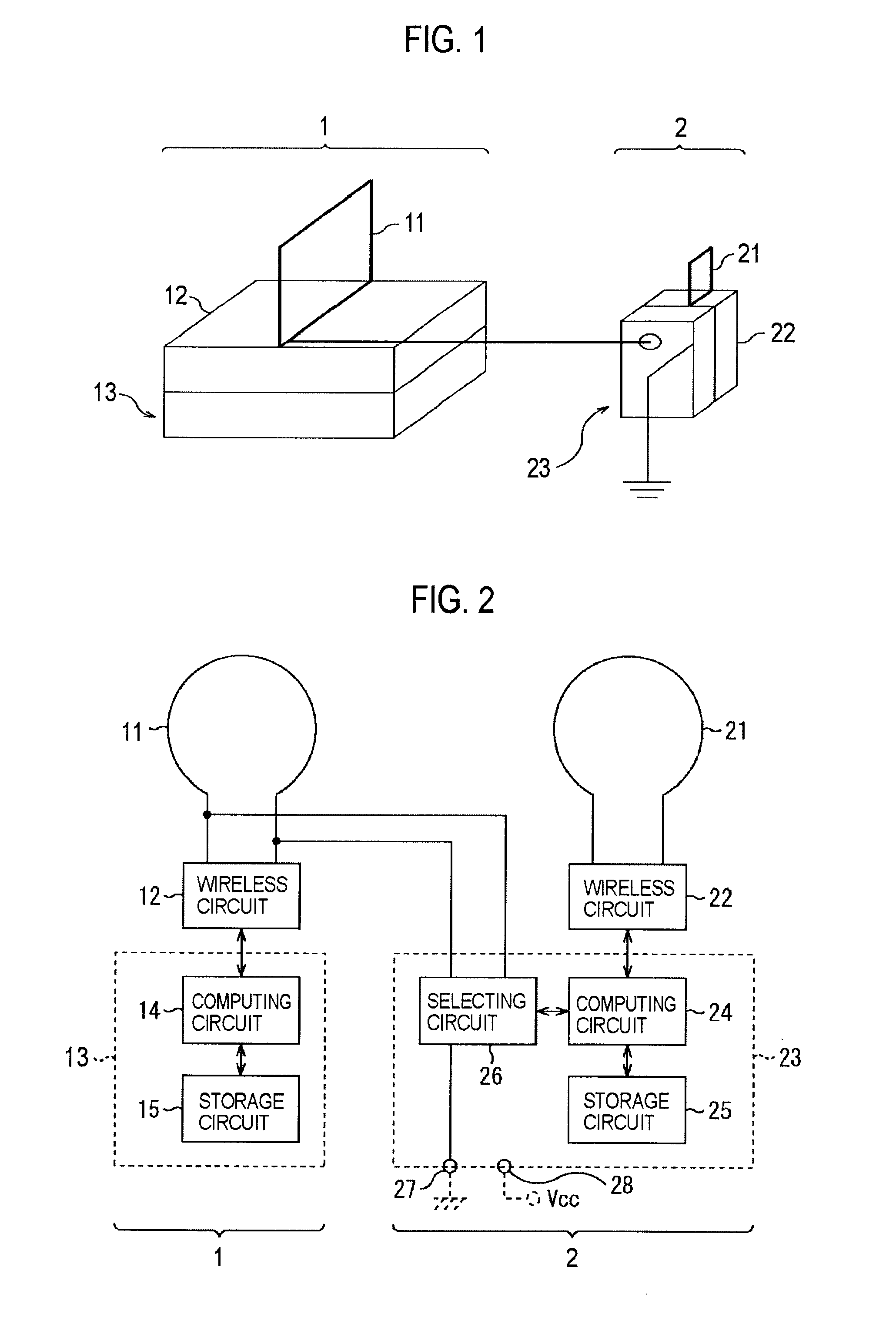
[0096]Description will be made regarding an embodiment of the present invention below with reference to the drawings. FIG. 1 is a perspective view schematically representing a semiconductor chip to which the present invention is applied. In FIG. 1, the semiconductor chip is made up of a signal processing block 1 and a control block 2, which are configured on a one-chip CMOS (Complementary Metal Oxide Semiconductor), for example. Accordingly, the semiconductor chip in FIG. 1 is a one-chip IC (Integrated Circuit) or an LSI (Large Scale Integration).

[0097]In the semiconductor chip in FIG. 1, signal terminals (pins) for inputting / outputting signals between the chip and outside of the chip can be provided. However, with the present embodiment, signal terminals are not provided on the semiconductor chip except for the power supply terminal and ground terminal for connecting to the power supply source and the ground (ground). In other words, a ground terminal 27 and power supply terminal 2...


PUM


Abstract

An IC chip allows first communication for performing communication with all of the other IC chips, and second communication for performing communication while restricting communication parties. That is to say, the IC chip performs sending / receiving signals with a new communication arrangement with both the first communication which is a broadcasting arrangement and the second communication which is a communicatory arrangement. This enables the function upgrading electronic equipment to be performed easily, and enables flexible signal processing with a new communication arrangement.

Description

CROSS-REFERENCE TO RELATED APPLICATIONS[0001]This application is a divisional of application Ser. No. 10 / 936,772 filed on Sep. 9, 2004 which claims to benefit of priority under 35 USC 119 to Japanese Application Number P2003-317710 filed on Sep. 10, 2003; Japanese Application Number P2003-317711 filed on Sep. 10, 2003, the entire contents of which are hereby incorporated by reference.BACKGROUND OF THE INVENTION[0002]1. Field of the Invention[0003]The present invention relates to a signal processing apparatus and signal processing method, program, and a recording medium, and more specifically, relates to a signal processing apparatus and signal processing method, program, and a recording medium which enable the function of electronic equipment to be upgraded easily, and enable flexible signal processing by performing communication according to a new arrangement.[0004]2. Description of the Related Art[0005]Audio and video equipment, such as television receivers or disk devices, commun...

Claims


Application Information

Patent Timeline
Patent Type & Authority Applications(United States)
IPC IPC(8): H04B1/18H04B1/40G06F9/00H04B1/66H04B7/00H04B7/10H04B7/24H04B7/26H04B17/00H04L29/00
CPCH04B7/10H04W4/06H04B1/0064H04B7/2621
Inventor KONDO, TETSUJIRONAKANISHI, TAKASHI
Owner SONY CORP
Why Eureka
Try Eureka