Hardened Memory Cell

a memory cell and hardened technology, applied in the field of memory cells, can solve the problems of reducing the speed of the cell, affecting the storage efficiency of the cell, and the loss of the information it is supposed to store, and achieve the effect of low surface cos

a memory cell and hardened technology, applied in the field of memory cells, can solve the problems of reducing the speed of the cell, affecting the storage efficiency of the cell, and the loss of the information it is supposed to store, and achieve the effect of low surface cos

US20080253180A1Active Publication Date: 2008-10-16IROC TECH

Image

  • Hardened Memory Cell
  • Hardened Memory Cell
  • Hardened Memory Cell

Examples


Embodiment Construction

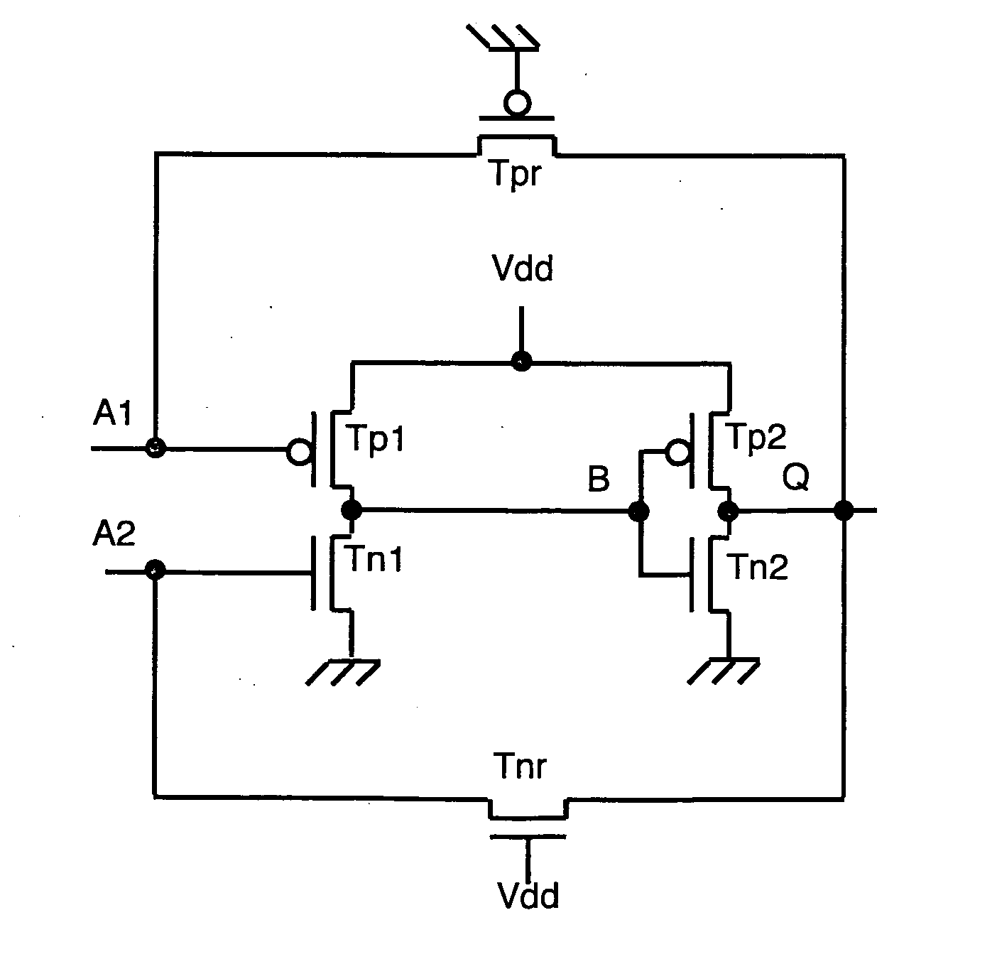
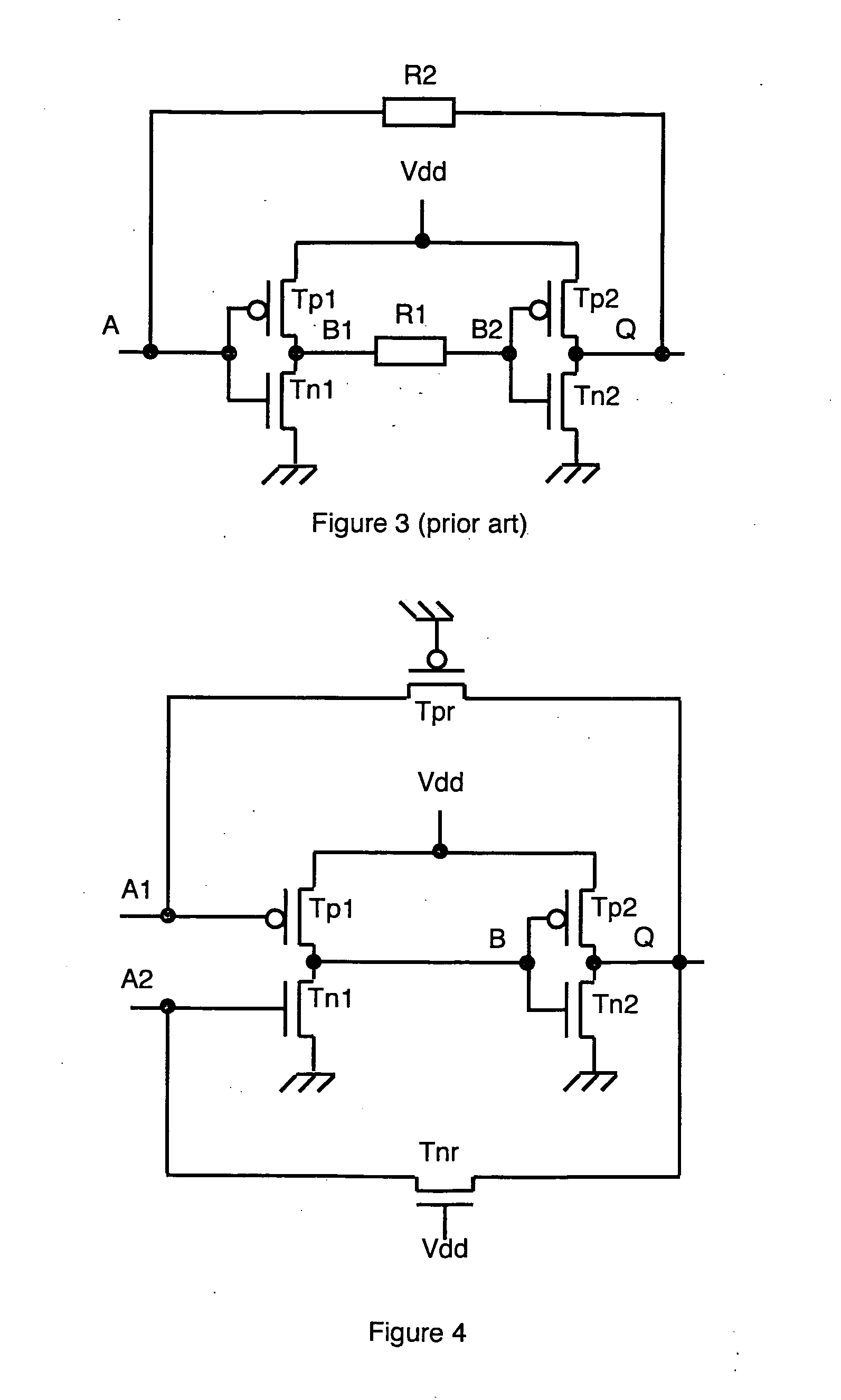
[0030]In the alternative illustrated in FIG. 4, the first inverter comprises two inputs A1 and A2 to which identical signals are applied. First and second long transistors Tpr and Tnr, respectively P-type and N-type, are connected in two distinct feedback loops, respectively between the output Q of the second inverter and the gates of the transistors Tp1 and Tn1 respectively constituting the first and second inputs A1 and A2 of the first inverter. The gates of transistors Tnr and Tpr are respectively connected to the supply voltage Vdd and to ground and these two transistors are consequently always turned on. Propagation of a transient error from output Q to inputs A1 and A2 is delayed by the resistors formed by transistors Tpr and Tnr.

[0031]Direct connection of the output of the 1st inverter (Tp1, Tn1) and of the input of the 2nd inverter (Tp2, Tn2) prevents an additional delay from being introduced in the write phase. Moreover, this embodiment does not introduce any additional ste...


PUM


Abstract

The memory cell comprises first and second inverter circuits, connected in a loop. First and second decoupling transistors, normally turned off outside the write phases, are respectively connected between an output of the second inverter circuit and first and second inputs of the first inverter circuit. The memory cell is thereby protected against transient disturbances due to ionizing particles. The gates of the decoupling transistors are preferably respectively connected to a supply voltage for the P-type decoupling transistors and grounded for the N-type decoupling transistors.

Description

BACKGROUND OF THE INVENTION[0001]The invention relates to a memory cell protected against transient disturbances.STATE OF THE ART[0002]As represented in FIG. 1, a memory cell conventionally comprises two loop-connected inverters. Thus, a first inverter 1 comprising an input A and an output B, a second inverter 2 is connected in a feedback loop. Its input is then connected to output B of the first inverter, whereas its output is connected to input A of first inverter 1. The information is stored in the two nodes (A and B) which connect the output of one inverter with the input of the other. The state of the output of an inverter is however determined by the state of its input. If this electric state is degraded because of leakage currents, the cell can lose the information it is supposed to store. This is not the case with a cell according to FIG. 1, for the output of each inverter is able to supply a current that is able to compensate the losses due to these leakage currents.[0003]H...

Claims


Application Information

Patent Timeline
16 Oct 2008
Publication
US20080253180A1
IPC
G11C11/412; H03K3/037
CPC
G11C11/412; H03K3/0375
Inventors
NICOLAIDIS, MICHEL; PEREZ, RENAUD