Solid-state imaging device for color imaging

a color image and imaging device technology, applied in the field of color image imaging solid-state imaging devices, can solve the problems of inability to capture color images, inability to reduce the quality of captured images due to the positional offset of sampling points, and in principle unavoidable, so as to improve light utilization efficiency and reduce image deterioration

Inactive Publication Date: 2009-04-30
FUJIFILM CORP
View PDF6 Cites 13 Cited by
  • Summary
  • Abstract
  • Description
  • Claims
  • Application Information

AI Technical Summary

Benefits of technology

[0018]According to the invention, signals of a plurality of colors for generating a color image can be detected by one opening, and members which thermally consume the light wastefully as in the case of color filters are not used, so that the light utilization efficiency is enhanced.
[0019]Furthermore, since spectral elements having trapezoidal openings are densely arranged on the light receiving surface of the solid-state imaging device, the configuration becomes such that two adjacent trapezoidal openings are configured to be entangled. Therefore, it becomes possible to reduce image deterioration due to the folded distortion even if optical low-pass filters are not used.

Problems solved by technology

For this reason, approximately two-thirds of the light incident upon one photodiode is absorbed by the color filter (for example, blue light and green light incident upon the red color filter are absorbed and converted to heat), so that, in principle, there is a problem in that the light utilization efficiency is low.
Hence, there is another problem in that a decline in the quality of the captured image due to the positional offset of sampling points is, in principle, unavoidable.

Method used


Image

  • Solid-state imaging device for color imaging
  • Solid-state imaging device for color imaging
  • Solid-state imaging device for color imaging

Examples


Embodiment Construction

[0049]Hereafter, a description will be given of the embodiments of the invention with reference to the accompanying drawings.

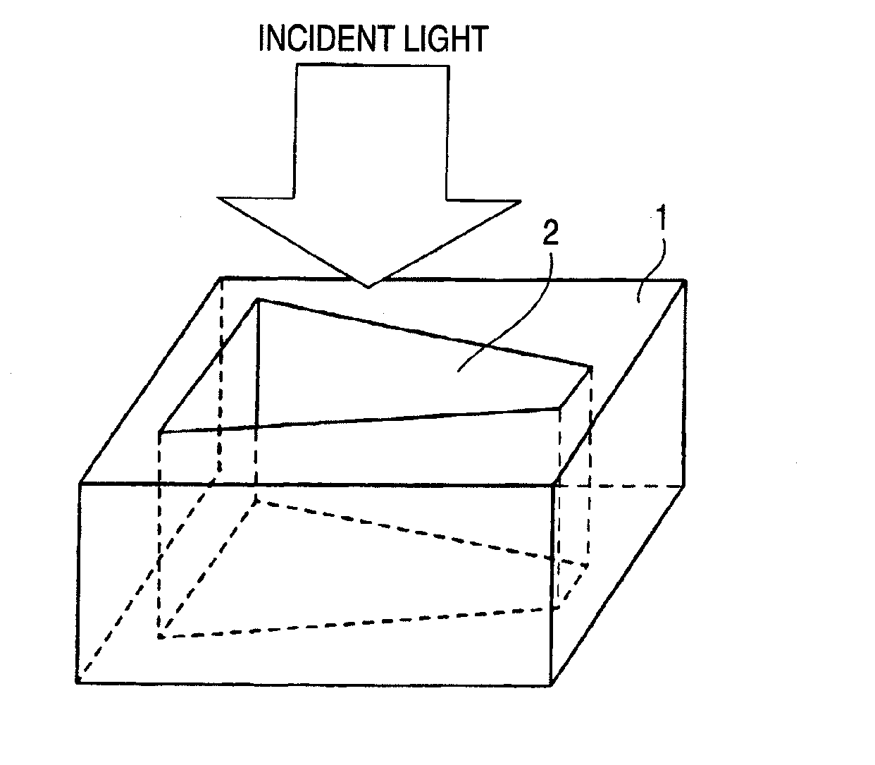
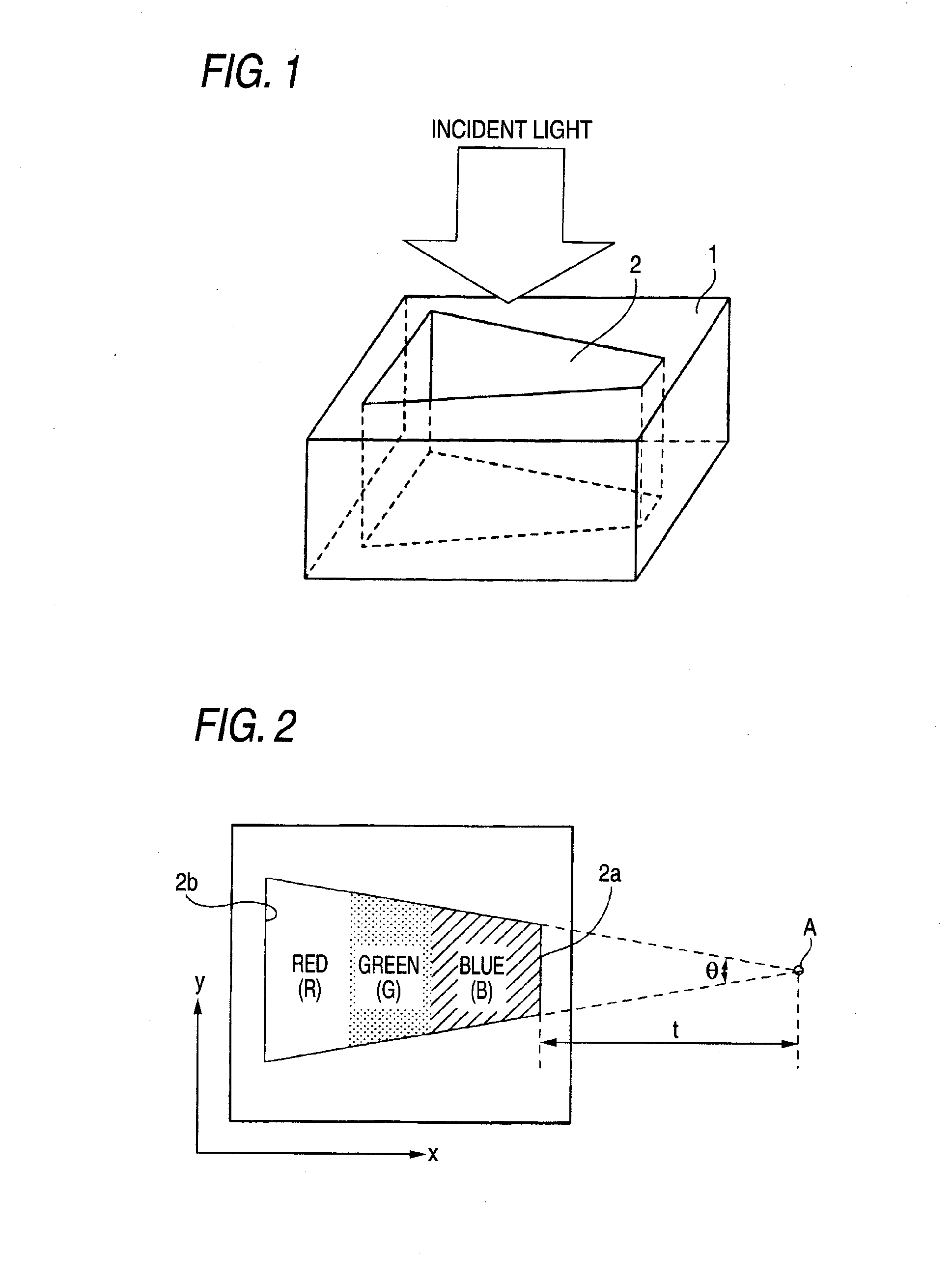
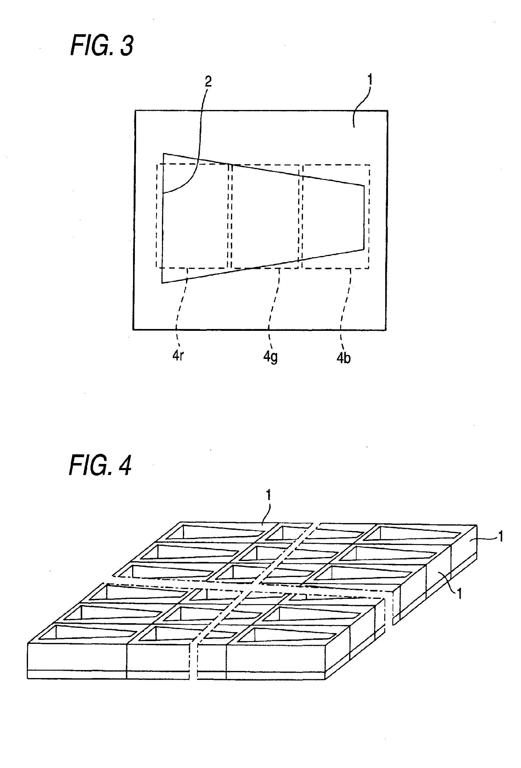
[0050]FIG. 1 is a perspective view of a spectral element which is used in a solid-state imaging device for capturing a color image in accordance with an embodiment of the invention. This spectral element 1 is formed of a thick metal plate in accordance with this embodiment, and in the illustrated example an opening 2 which is trapezoidal in a top view is provided penetratingly from an upper surface to a lower surface.

[0051]Inner side surfaces of the opening 2 may be provided vertically with respect to upper and lower surfaces, or may be provided in an inclined manner to provide a tapered opening such that the opening in the lower surface becomes smaller with a similar figure with respect to the opening in the upper surface.

[0052]The reason that the spectral element 1 is formed of a thick metal plate is that it is necessary to provide a sufficient length (thick...


PUM


Abstract

A solid-state imaging device includes a plurality of photoelectric conversion elements provided at a surface portion of a semiconductor substrate by being arranged in a form of a two-dimensional array, spectral elements each provided on a number of the photoelectric conversion elements which are arranged linearly, a trapezoidal opening which is longitudinally elongated in a direction from a base toward an upper side thereof and which introduces incident light to the number of the photoelectric conversion elements being provided in each of the spectral elements, so as to cause spectral separation in the longitudinal direction by interference between the incident light and light reflected on inner side surfaces of the trapezoidal opening and a signal reading unit for reading a signal which is detected by each of the number of the photoelectric conversion elements arranged in the longitudinal direction by receiving the light incident through the trapezoidal opening.

Description

CROSS-REFERENCE TO RELATED APPLICATIONS[0001]This application claims the benefit of Japanese Patent Application JP 2007-280599, filed Oct. 29, 2007, the entire content of which is hereby incorporated by reference, the same as if set forth at length.FIELD OF THE INVENTION[0002]The present invention relates to a solid-state imaging device for capturing a color image, and more particularly to a solid-state imaging device which is capable of capturing a color image without using color filters.BACKGROUND OF THE INVENTION[0003]As solid-state imaging devices for capturing color images, single-plate type imaging devices such as a complementary metal oxide semiconductor (CMOS) type, a charge coupled device (CCD) type, and the like are conventionally known. As described in JP-A-2007-180157 (corresponding to US2007 / 0145241A1), for example, these solid-state imaging devices are structured such that a plurality of photodiodes, i.e., photoelectric conversion elements, are formed at the surface po...

Claims


Application Information

Patent Timeline
Patent Type & Authority Applications(United States)
IPC IPC(8): H04N5/335H01L27/14H04N5/369H04N5/374H04N9/07
CPCG02B5/008G02B5/201H04N9/097H04N9/045H04N9/083H04N5/2254H04N23/84H04N25/17H04N9/03H04N23/16
Inventor NISHIDA, YOSHIYASUKOBAYASHI, HIROKAZUIWATA, MITSURUFURUTA, YOSHINORIKUSUDA, DAISUKE
Owner FUJIFILM CORP
Why Eureka
Try Eureka